- 您現在的位置:買賣IC網 > PDF目錄382679 > TPS62046DRC (Texas Instruments, Inc.) Programmable Logic Controller; Leaded Process Compatible:No; Peak Reflow Compatible (260 C):No RoHS Compliant: No PDF資料下載
參數資料
| 型號: | TPS62046DRC |
| 廠商: | Texas Instruments, Inc. |
| 英文描述: | Programmable Logic Controller; Leaded Process Compatible:No; Peak Reflow Compatible (260 C):No RoHS Compliant: No |
| 中文描述: | 可編程邏輯控制器;無鉛,不支持260℃峰值回流焊溫度;符合RoHS認證 |
| 文件頁數: | 16/21頁 |
| 文件大小: | 372K |
| 代理商: | TPS62046DRC |
SLVS463A JUNE 2003 REVISED OCTOBER 2003
www.ti.com
16
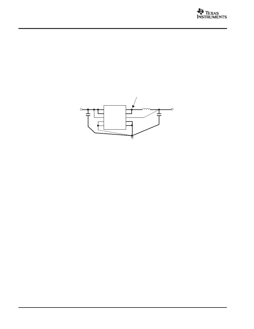
Layout Considerations
For all switching power supplies, the layout is an important step in the design especially at high peak currents and
switching frequencies. If the layout is not carefully done, the regulator might show stability problems as well as EMI
problems. Therefore, use wide and short traces for the main current paths as indicated in bold in Figure 16. These
traces should be routed first. The input capacitor should be placed as close as possible to the IC pins as well as the
inductor and output capacitor. The feedback resistor network should be routed away from the inductor and switch
node to minimize noise and magnetic interference. To further minimize noise from coupling into the feedback network
and feedback pin, the ground plane or ground traces should be used for shielding. A common ground plane or a star
ground as shown below should be used. This becomes very important especially at high switching frequencies of
1.25 MHz.
VIN
VIN
EN
MODE
GND
SW
SW
FB
PGND
PGND
2
3
1
6
4
9
10
5
7
8
TPS6204x
C3
22
μ
F
VI
L1
10
μ
H
C2
22
μ
F
VO
The Switch Node Must Be
Kept as Small as Possible
Figure 16. Layout Diagram
THERMAL INFORMATION
One of the most influential components on the thermal performance of a package is board design. In order to take
full advantage of the heat dissipating abilities of the PowerPAD packages, a board should be used that acts similar
to a heat sink and allows for the use of the exposed (and solderable), deep downset pad. For further information
please refer to Texas Instruments application note (SLMA002)
PowerPAD Thermally Enhanced Package
.
The PowerPAD of the 10-pin MSOP package has an area of 1,52 mm
×
1,79 mm (
±
0,05 mm) and must be soldered
to the PCB to lower the thermal resistance. Thermal vias to the next layer further reduce the thermal resistance.
相關PDF資料 |
PDF描述 |
|---|---|
| TPS62043DRC | IDC Connector |
| TPS62040DRC | 1.2 A/1.25 MHZ, HIGH EFFICIENCY STEP DOWN CONVERTER |
| TPS62042DRC | 1.2 A/1.25 MHZ, HIGH EFFICIENCY STEP DOWN CONVERTER |
| TPS62044DRC | 1.2 A/1.25 MHZ, HIGH EFFICIENCY STEP DOWN CONVERTER |
| TPS62224DDC | 400-mA, 1.25-MHz, HIGH-EFFICIENCY, STEP-DOWN CONVERTER IN THIN-SOT23 |
相關代理商/技術參數 |
參數描述 |
|---|---|
| TPS62046DRCR | 功能描述:直流/直流開關調節器 3.3V Out/1.2A Hi-Eff Step-Down Converter RoHS:否 制造商:International Rectifier 最大輸入電壓:21 V 開關頻率:1.5 MHz 輸出電壓:0.5 V to 0.86 V 輸出電流:4 A 輸出端數量: 最大工作溫度: 安裝風格:SMD/SMT 封裝 / 箱體:PQFN 4 x 5 |
| TPS62046DRCRG4 | 功能描述:直流/直流開關調節器 3.3V Out/1.2A Hi-Eff Step-Down Converter RoHS:否 制造商:International Rectifier 最大輸入電壓:21 V 開關頻率:1.5 MHz 輸出電壓:0.5 V to 0.86 V 輸出電流:4 A 輸出端數量: 最大工作溫度: 安裝風格:SMD/SMT 封裝 / 箱體:PQFN 4 x 5 |
| TPS62046EVM-229 | 功能描述:電源管理IC開發工具 TPS62046-229 Eval Mod RoHS:否 制造商:Maxim Integrated 產品:Evaluation Kits 類型:Battery Management 工具用于評估:MAX17710GB 輸入電壓: 輸出電壓:1.8 V |
| TPS62050DGS | 功能描述:直流/直流開關調節器 Adj 800mA 10V Vin Step-Down Converter RoHS:否 制造商:International Rectifier 最大輸入電壓:21 V 開關頻率:1.5 MHz 輸出電壓:0.5 V to 0.86 V 輸出電流:4 A 輸出端數量: 最大工作溫度: 安裝風格:SMD/SMT 封裝 / 箱體:PQFN 4 x 5 |
| TPS62050DGSG4 | 功能描述:直流/直流開關調節器 Adj 800mA 10V Vin Step-Down Converter RoHS:否 制造商:International Rectifier 最大輸入電壓:21 V 開關頻率:1.5 MHz 輸出電壓:0.5 V to 0.86 V 輸出電流:4 A 輸出端數量: 最大工作溫度: 安裝風格:SMD/SMT 封裝 / 箱體:PQFN 4 x 5 |
發布緊急采購,3分鐘左右您將得到回復。