- 您現在的位置:買賣IC網 > PDF目錄98284 > TPS62230DRYR (TEXAS INSTRUMENTS INC) 1.22 A SWITCHING REGULATOR, 3800 kHz SWITCHING FREQ-MAX, PDSO6 PDF資料下載
參數資料
| 型號: | TPS62230DRYR |
| 廠商: | TEXAS INSTRUMENTS INC |
| 元件分類: | 穩壓器 |
| 英文描述: | 1.22 A SWITCHING REGULATOR, 3800 kHz SWITCHING FREQ-MAX, PDSO6 |
| 封裝: | 1 X 1.50 MM, 0.60 MM HEIGHT, GREEN, PLASTIC, MO-287UFAD, SON-6 |
| 文件頁數: | 1/34頁 |
| 文件大小: | 1181K |
| 代理商: | TPS62230DRYR |
當前第1頁第2頁第3頁第4頁第5頁第6頁第7頁第8頁第9頁第10頁第11頁第12頁第13頁第14頁第15頁第16頁第17頁第18頁第19頁第20頁第21頁第22頁第23頁第24頁第25頁第26頁第27頁第28頁第29頁第30頁第31頁第32頁第33頁第34頁
V
IN
GND
V
OUT
C
1
C2
L1
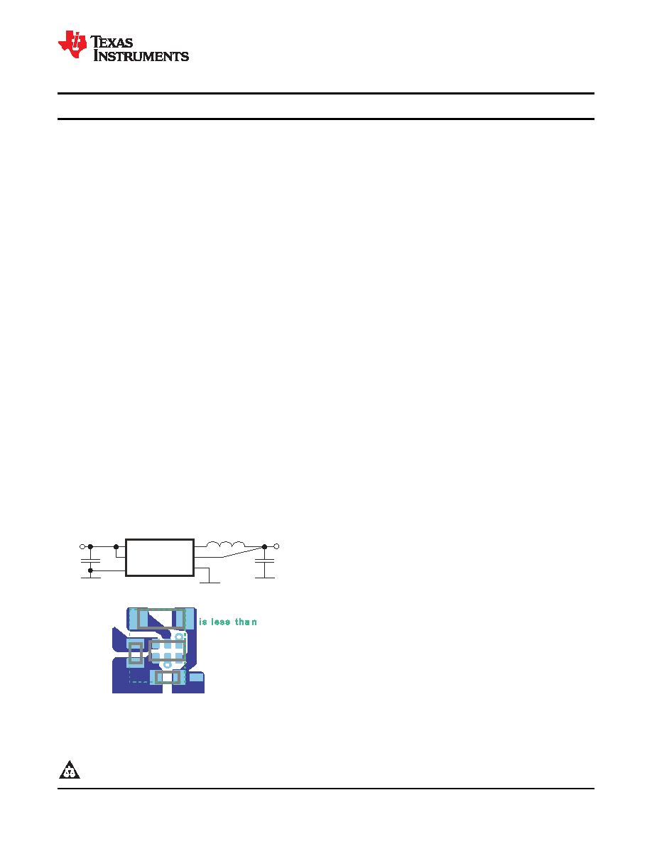
Totalarea
12mm
1.8V
V
OUT
2.05V-6V
V
IN
2.2
F
m
C
IN
L
1/2.2
H
m
C
4.7
F
OUT
m
TPS62231
VIN
EN
MODE
SW
FB
GND
TPS62230, TPS62231, TPS62232, TPS62233, TPS62234, TPS62235, TPS62236
TPS62237, TPS62238, TPS62239, TPS622310, TPS622311, TPS622312
TPS622313, TPS622314, TPS622315, TPS622316, TPS622317, TPS622318
www.ti.com
SLVS941E – APRIL 2009 – REVISED DECEMBER 2010
2 MHz / 3 MHz Ultra Small Step Down Converter in 1x1.5 SON Package
1
FEATURES
DESCRIPTION
2 MHz / 3 MHz Switch Frequency
Up to 94% Efficiency
The TPS6223X device family is a high frequency
synchronous step down DC-DC converter optimized
Output Peak Current up to 500mA
for battery powered portable applications. It supports
Excellent AC and Transient Load Regulation
up to 500mA output current and allows the use of tiny
High PSRR (up to 90dB)
and low cost chip inductors and capacitors.
Small External Output Filter Components 1mH/
With a wide input voltage range of 2.05V to 6V the
4.7mF
device supports applications powered by Li-Ion
batteries with extended voltage range. The minimum
VIN range from 2.05V to 6V
input voltage of 2.05V allows as well the operation
Optimized Power Save Mode For Low Output
from Li-primary or two alkaline batteries. Different
Ripple Voltage
fixed output voltage versions are available from 1.0V
Forced PWM Mode Operation
to 3.3V.
Typ. 22 mA Quiescent Current
The TPS6223X series features switch frequency up
100% Duty Cycle for Lowest Dropout
to 3.8MHz. At medium to heavy loads, the converter
operates in PWM mode and automatically enters
Small 1 × 1.5 × 0.6mm3 SON Package
Power Save Mode operation at light load currents to
12 mm2 Minimum Solution Size
maintain high efficiency over the entire load current
Supports 0.6 mm Maximum Solution Height
range.
Soft Start with typ. 100ms Start Up Time
Because
of
its
excellent
PSRR
and
AC
load
regulation performance, the device is also suitable to
APPLICATIONS
replace linear regulators to obtain better power
LDO Replacement
conversion efficiency.
Portable Audio, Portable Media
The Power Save Mode in TPS6223X reduces the
Cell Phones
quiescent current consumption down to 22mA during
light load operation. It is optimized to achieve very
Low Power Wireless
low output voltage ripple even with small external
Low Power DSP Core Supply
component and features excellent ac load regulation.
Digital Cameras
For very noise sensitive applications, the device can
be forced to PWM Mode operation over the entire
load range by pulling the MODE pin high. In the
shutdown mode, the current consumption is reduced
to less than 1mA. The TPS6223X is available in a 1 ×
1.5mm2 6 pin SON package.
1
Please be aware that an important notice concerning availability, standard warranty, and use in critical applications of Texas
Instruments semiconductor products and disclaimers thereto appears at the end of this data sheet.
PRODUCTION DATA information is current as of publication date.
Copyright 2009–2010, Texas Instruments Incorporated
Products conform to specifications per the terms of the Texas
Instruments standard warranty. Production processing does not
necessarily include testing of all parameters.
相關PDF資料 |
PDF描述 |
|---|---|
| TPS62250DRVR | SWITCHING REGULATOR, 2500 kHz SWITCHING FREQ-MAX, PDSO6 |
| TPS62260IDRVRQ1 | SWITCHING REGULATOR, PDSO6 |
| TPS62260QDRVRQ1 | SWITCHING REGULATOR, PDSO6 |
| TPS62261DRV | 1.2 A SWITCHING REGULATOR, 2500 kHz SWITCHING FREQ-MAX, PDSO6 |
| TPS62262DRV | 1.2 A SWITCHING REGULATOR, 2500 kHz SWITCHING FREQ-MAX, PDSO6 |
相關代理商/技術參數 |
參數描述 |
|---|---|
| TPS62230DRYT | 功能描述:直流/直流開關調節器 3 MHz Ultra Small Step Down Converter RoHS:否 制造商:International Rectifier 最大輸入電壓:21 V 開關頻率:1.5 MHz 輸出電壓:0.5 V to 0.86 V 輸出電流:4 A 輸出端數量: 最大工作溫度: 安裝風格:SMD/SMT 封裝 / 箱體:PQFN 4 x 5 |
| TPS62230DRYT | 制造商:Texas Instruments 功能描述:DC/DC Converter IC 制造商:Texas Instruments 功能描述:IC, STEP-DOWN CONVERTER, SON-6 |
| TPS62230EVM-370 | 功能描述:電源管理IC開發工具 TPS62230EVM-370 Eval Mod RoHS:否 制造商:Maxim Integrated 產品:Evaluation Kits 類型:Battery Management 工具用于評估:MAX17710GB 輸入電壓: 輸出電壓:1.8 V |
| TPS62230EVM-574 | 功能描述:電源管理IC開發工具 TPS62230 Eval Mod RoHS:否 制造商:Maxim Integrated 產品:Evaluation Kits 類型:Battery Management 工具用于評估:MAX17710GB 輸入電壓: 輸出電壓:1.8 V |
| TPS622310DRYR | 功能描述:直流/直流開關轉換器 3MHz 500mA Step- Down Converter RoHS:否 制造商:STMicroelectronics 最大輸入電壓:4.5 V 開關頻率:1.5 MHz 輸出電壓:4.6 V 輸出電流:250 mA 輸出端數量:2 最大工作溫度:+ 85 C 安裝風格:SMD/SMT |
發布緊急采購,3分鐘左右您將得到回復。