- 您現在的位置:買賣IC網 > PDF目錄382680 > TPS62300DRC (Texas Instruments, Inc.) 500-mA, 3-MHz SYNCHRONOUS STEP-DOWN CONVERTER IN CHIP SCALE PACKAGING PDF資料下載
參數資料
| 型號: | TPS62300DRC |
| 廠商: | Texas Instruments, Inc. |
| 英文描述: | 500-mA, 3-MHz SYNCHRONOUS STEP-DOWN CONVERTER IN CHIP SCALE PACKAGING |
| 中文描述: | 500毫安,3 MHz的同步降壓轉換器芯片級封裝 |
| 文件頁數: | 19/31頁 |
| 文件大小: | 1635K |
| 代理商: | TPS62300DRC |
第1頁第2頁第3頁第4頁第5頁第6頁第7頁第8頁第9頁第10頁第11頁第12頁第13頁第14頁第15頁第16頁第17頁第18頁當前第19頁第20頁第21頁第22頁第23頁第24頁第25頁第26頁第27頁第28頁第29頁第30頁第31頁
www.ti.com
INPUT CAPACITOR SELECTION
Because of the nature of the buck converter having a pulsating input current, a low ESR input capacitor is
required to prevent large voltage transients that can cause misbehavior of the device or interferences with other
circuits in the system. For most applications, a 2.2-
μ
F or 4.7-
μ
F capacitor is sufficient.
Take care when using only ceramic input capacitors. When a ceramic capacitor is used at the input and the
power is being supplied through long wires, such as from a wall adapter, a load step at the output can induce
ringing at the VIN pin. This ringing can couple to the output and be mistaken as loop instability or could even
damage the part.
CHECKING LOOP STABILITY
The first step of circuit and stability evaluation is to look from a steady-state perspective at the following signals:
Switching node, SW
Inductor current, I
L
Output ripple voltage, V
O(AC)
These are the basic signals that need to be measured when evaluating a switching converter. When the
switching waveform shows large duty cycle jitter or the output voltage or inductor current shows oscillations, the
regulation loop may be unstable. This is often a result of board layout and/or L-C combination.
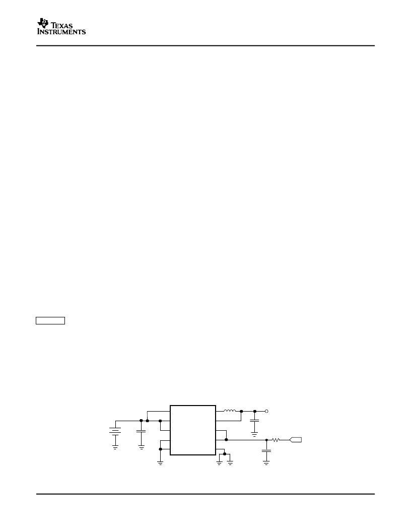
PROGRAMMING THE OUTPUT VOLTAGE WITH A DAC
On TPS62300 and TPS62320 devices, the output voltage can be dynamically programmed to any voltage
between 0.6 V and V
I
(or 5.4 V whichever is lower) with an external DAC driving the ADJ and FB pins (see
Figure 33
). The output voltage is then equal to A
(PT)
x V
(DAC)
with a
Power Train
amplification A
(PT)
typical = 1.5.
When the output voltage is driven low, the converter reduces its output quickly in forced PWM mode, boosting
the output energy back to the input. If the input is not connected to a low-impedance source capable of absorbing
the energy, the input voltage can rise above the absolute maximum voltage of the part and get damaged. The
faster V
O
is commanded low, the higher is the voltage spike at the input.
For best results, ramp the ADJ/FB signal as slow as the application allows. To avoid over-slew of the regulation
loop of the converter, avoid abrupt changes in output voltage of > 300 mV/
μ
s (depending on V
, output voltage
step size and L/C combination). If ramp control is unavailable, an RC filter can be inserted between the DAC
output and ADJ/FB pins to slow down the control signal.
AVIN
VIN
SW
TPS62300
L
ADJ
PGND
AGND
VOUT
EN
MODE/SYNC
A
A
FB
A
1
2
3
8
7
10
6
4
5
9
V
O
=1.5xV
(
D
A
C
)
V
(
D
A
C
)
C
O
R
F
C
F
C
I
V
I
10k
W
TPS62300, TPS62301, TPS62302
TPS62303, TPS62305, TPS62311
TPS62313, TPS62320, TPS62321
SLVS528B–JULY 2004–REVISED JUNE 2005
As a next step in the evaluation of the regulation loop, the load transient response is tested. The time between
the application of the load transient and the turn on of the P-channel MOSFET, the output capacitor must supply
all of the current required by the load. V
O
immediately shifts by an amount equal to
I
(LOAD)
x ESR, where ESR
is the effective series resistance of C
O
.
I
(LOAD)
begins to charge or discharge C
O
generating a feedback error
signal used by the regulator to return V
O
to its steady-state value.
During this recovery time, V
O
can be monitored for settling time, overshoot or ringing that helps judge the
converter’s stability. Without any ringing, the loop has usually more than 45
°
of phase margin.
Because the damping factor of the circuitry is directly related to several resistive parameters (e.g., MOSFET
r
DS(on)
) that are temperature dependant, the loop stability analysis has to be done over the input voltage range,
load current range, and temperature range.
Figure 33. Filtering the DAC Voltage
19
相關PDF資料 |
PDF描述 |
|---|---|
| TPS62300YZD | 500-mA, 3-MHz SYNCHRONOUS STEP-DOWN CONVERTER IN CHIP SCALE PACKAGING |
| TPS62301DRC | 500-mA, 3-MHz SYNCHRONOUS STEP-DOWN CONVERTER IN CHIP SCALE PACKAGING |
| TPS62301YZD | 500-mA, 3-MHz SYNCHRONOUS STEP-DOWN CONVERTER IN CHIP SCALE PACKAGING |
| TPS62302DRC | 500-mA, 3-MHz SYNCHRONOUS STEP-DOWN CONVERTER IN CHIP SCALE PACKAGING |
| TPS62302YZD | 500-mA, 3-MHz SYNCHRONOUS STEP-DOWN CONVERTER IN CHIP SCALE PACKAGING |
相關代理商/技術參數 |
參數描述 |
|---|---|
| TPS62300DRCR | 功能描述:直流/直流開關調節器 Adj 500-mA 3-MHz Step-Down Converter RoHS:否 制造商:International Rectifier 最大輸入電壓:21 V 開關頻率:1.5 MHz 輸出電壓:0.5 V to 0.86 V 輸出電流:4 A 輸出端數量: 最大工作溫度: 安裝風格:SMD/SMT 封裝 / 箱體:PQFN 4 x 5 |
| TPS62300DRCR | 制造商:Texas Instruments 功能描述:DC/DC CONVERTER IC 制造商:Texas Instruments 功能描述:IC, SYNC STEP-DOWN CONVERTER, SON-10 |
| TPS62300DRCRG4 | 功能描述:直流/直流開關調節器 Adj 500-mA 3-MHz Step-Down Converter RoHS:否 制造商:International Rectifier 最大輸入電壓:21 V 開關頻率:1.5 MHz 輸出電壓:0.5 V to 0.86 V 輸出電流:4 A 輸出端數量: 最大工作溫度: 安裝風格:SMD/SMT 封裝 / 箱體:PQFN 4 x 5 |
| TPS62300DRCT | 制造商:Texas Instruments 功能描述:CONV DC-DC SGL-OUT STEP DOWN 10PIN SON EP - Tape and Reel |
| TPS62300EVM-085 | 功能描述:電源管理IC開發工具 TPS62300-085 Eval Mod RoHS:否 制造商:Maxim Integrated 產品:Evaluation Kits 類型:Battery Management 工具用于評估:MAX17710GB 輸入電壓: 輸出電壓:1.8 V |
發布緊急采購,3分鐘左右您將得到回復。