- 您現在的位置:買賣IC網 > PDF目錄98284 > TPS62510DRCT (TEXAS INSTRUMENTS INC) 1.5 A SWITCHING REGULATOR, 1700 kHz SWITCHING FREQ-MAX, PDSO10 PDF資料下載
參數資料
| 型號: | TPS62510DRCT |
| 廠商: | TEXAS INSTRUMENTS INC |
| 元件分類: | 穩壓器 |
| 英文描述: | 1.5 A SWITCHING REGULATOR, 1700 kHz SWITCHING FREQ-MAX, PDSO10 |
| 封裝: | 3 X 3 MM, PLASTIC, SON-10 |
| 文件頁數: | 18/24頁 |
| 文件大小: | 1063K |
| 代理商: | TPS62510DRCT |
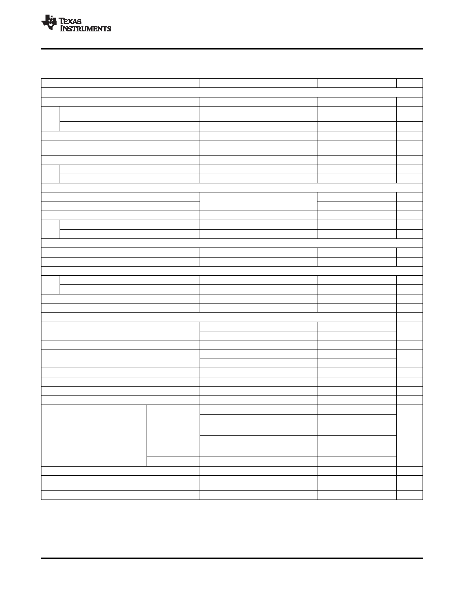
ELECTRICAL CHARACTERISTICS
www.ti.com ................................................................................................................................................................ SLVS651A – MAY 2006 – REVISED JULY 2009
VIN = 3.3 V, OVT = EN = VIN, MODE = GND, TA = –40°C to 85°C, typical values are at TA = 25°C (unless otherwise noted)
PARAMETER
TEST CONDITIONS
MIN
TYP
MAX
UNIT
SUPPLY CURRENT
VI
Input voltage range
1.8
3.8
V
Power Save Mode quiescent current
FB = FB nominal + 5%, MODE = low
22
30
A
AVIN + PVIN
I(q)
PWM Mode quiescent current into AVIN
MODE = high
4.4
5
mA
I(SD)
Shutdown current into PVIN + AVIN
EN = low, SW = GND
0.1
5
A
UVL
Undervoltage lockout threshold on AVIN
V(AVIN) falling
(1)
1.55
1.58
V
O
Undervoltage lockout hysteresis
150
mV
Thermal shutdown threshold
Increasing junction temperature
160
°C
T(SD)
Thermal shutdown hysteresis
20
°C
CONTROL SIGNALS EN, MODE
VIH
High level input voltage
1.2
V
VI = 1.8 V to 3.8 V
VIL
Low level input voltage
0.4
V
IIB
Input bias current
0.01
0.1
A
MODE synchronization range
1.15
2.25
MHz
f(sync)
Duration of high or low level for synchronization signal(2)
75
ns
OUTPUT VOLTAGE TRACKING (OVT)
IIB
Input bias current
0.001
0.05
A
VOS
OVT offset voltage
VOS = V(OVT) - V(FB), 0.1 V < V(OVT) < 0.5 V
-15
15
mV
POWER GOOD (PG)
Power Good threshold
Feedback voltage rising
-7% VO
-5% VO
-3% VO
V
V(th)
Power Good Hysteresis
2% VO
7% VO
V
VOL
Low level voltage
I(PG) = 1 mA
0.3
V
Ilkg
Power Good leakage current
V(PG) = 3.8 V
1
100
nA
OUTPUT
VI = V(GS) = 1.8 V
330
rDS(on) P-channel MOSFET on-resistance
m
VI = V(GS) = 3.3 V
120
170
Ilkg
P-channel leakage current
VI = 3.6 V
10
A
VI = V(GS) = 1.8 V
200
rDS(on) N-channel MOSFET on-resistance
m
VI = V(GS) = 3.3 V
80
130
Ilkg
N-channel leakage current
V(DS) = 3.6 V
10
A
IF
Forward current limit (P- and N-channel)
1.8 V < VI < 3.8 V
1.75
2.00
2.25
A
fs
Oscillator frequency
MODE = high
1.3
1.5
1.7
MHz
Vref
Reference voltage
0.6
V
VI = (VO + 0.3 V) to 3.8 V ;
-2%
5%
VI = (VO + 0.2 V) to 3.8 V; VO= 1.8V,
(4)
C2 = 15 F, L1= 2.1 H (effective values),
-2%
2.5%
PFM operation
IOUT = 0mA to 150mA
VFB
Feedback voltage (3)
VI = (VO + 0.3 V) to 3.8 V; VO= 2.5V,
(4)
C2 = 15 F, L1= 2.1 H (effective values),
-1.3%
2.3%
IOUT = 0mA to 150mA
PWM operation
VI = VO + 0.3 V
-1
1
IFB
Feedback bias current
V(FB) = 0.6 V, EN = high
0.001
0.05
A
VI = VO + 0.3 V (min 1.8 V) to 3.8 V;
Line Regulation
0
%/V
IO = 800 mA
Load Regulation
IO = 10 mA to 1500 mA, PWM Mode
0.1
%/A
(1)
The undervoltage lockout threshold is detected at the AVIN pin. Current through the RC filter causes a UVLO trip at higher VI
(2)
The minimum and maximum duty cycle applied to the MODE pin is calculated as:
D(min) = 75 ns × f(sync) and D(max) = 1 - 75 ns × f(sync).
(3)
When using the output voltage tracking function, the feedback regulates to the voltage applied to OVT as long as the OVT < 0.6 V.
(4)
Min/Max values established by characterization and not production tested. Includes line and load regulation in PFM Mode operation. For
the measurements, a proper PCB layout and usage of recommended inductors and capacitors are essential.
Copyright 2006–2009, Texas Instruments Incorporated
3
Product Folder Link(s): TPS62510
相關PDF資料 |
PDF描述 |
|---|---|
| TPS62510DRC | 1.5 A SWITCHING REGULATOR, 1700 kHz SWITCHING FREQ-MAX, PDSO10 |
| TPS62562DRVR | 0.6 A SWITCHING REGULATOR, 2250 kHz SWITCHING FREQ-MAX, PDSO6 |
| TPS62590DRVT | 1 A SWITCHING REGULATOR, 2250 kHz SWITCHING FREQ-MAX, PDSO6 |
| TPS62601YFFT | 1.1 A SWITCHING REGULATOR, 6600 kHz SWITCHING FREQ-MAX, BGA6 |
| TPS62660YFF | 1.75 A SWITCHING REGULATOR, 6600 kHz SWITCHING FREQ-MAX, BGA6 |
相關代理商/技術參數 |
參數描述 |
|---|---|
| TPS62510DRCT | 制造商:Texas Instruments 功能描述:DC/DC Converter (DC-DC) / Switching Regu |
| TPS62510DRCTG4 | 功能描述:直流/直流開關調節器 Adj. 97% Efficient 1.5A Buck Converter RoHS:否 制造商:International Rectifier 最大輸入電壓:21 V 開關頻率:1.5 MHz 輸出電壓:0.5 V to 0.86 V 輸出電流:4 A 輸出端數量: 最大工作溫度: 安裝風格:SMD/SMT 封裝 / 箱體:PQFN 4 x 5 |
| TPS62510EVM-168 | 功能描述:電源管理IC開發工具 BUCK CONVERTER RoHS:否 制造商:Maxim Integrated 產品:Evaluation Kits 類型:Battery Management 工具用于評估:MAX17710GB 輸入電壓: 輸出電壓:1.8 V |
| TPS62560DRVR | 功能描述:直流/直流開關調節器 2.25MHz 600mA Step- Down Cnvrtr RoHS:否 制造商:International Rectifier 最大輸入電壓:21 V 開關頻率:1.5 MHz 輸出電壓:0.5 V to 0.86 V 輸出電流:4 A 輸出端數量: 最大工作溫度: 安裝風格:SMD/SMT 封裝 / 箱體:PQFN 4 x 5 |
| TPS62560DRVRG4 | 功能描述:直流/直流開關調節器 90%Efficient Synch Boost Converter RoHS:否 制造商:International Rectifier 最大輸入電壓:21 V 開關頻率:1.5 MHz 輸出電壓:0.5 V to 0.86 V 輸出電流:4 A 輸出端數量: 最大工作溫度: 安裝風格:SMD/SMT 封裝 / 箱體:PQFN 4 x 5 |
發布緊急采購,3分鐘左右您將得到回復。