- 您現(xiàn)在的位置:買賣IC網(wǎng) > PDF目錄98285 > TPS65161BPWP (TEXAS INSTRUMENTS INC) SWITCHING REGULATOR, 900 kHz SWITCHING FREQ-MAX, PDSO28 PDF資料下載
參數(shù)資料
| 型號: | TPS65161BPWP |
| 廠商: | TEXAS INSTRUMENTS INC |
| 元件分類: | 穩(wěn)壓器 |
| 英文描述: | SWITCHING REGULATOR, 900 kHz SWITCHING FREQ-MAX, PDSO28 |
| 封裝: | PLASTIC, TSSOP-28 |
| 文件頁數(shù): | 32/34頁 |
| 文件大小: | 847K |
| 代理商: | TPS65161BPWP |
第1頁第2頁第3頁第4頁第5頁第6頁第7頁第8頁第9頁第10頁第11頁第12頁第13頁第14頁第15頁第16頁第17頁第18頁第19頁第20頁第21頁第22頁第23頁第24頁第25頁第26頁第27頁第28頁第29頁第30頁第31頁當(dāng)前第32頁第33頁第34頁
www.ti.com ............................................................................................................................................... SLVS617D – APRIL 2006 – REVISED SEPTEMBER 2009
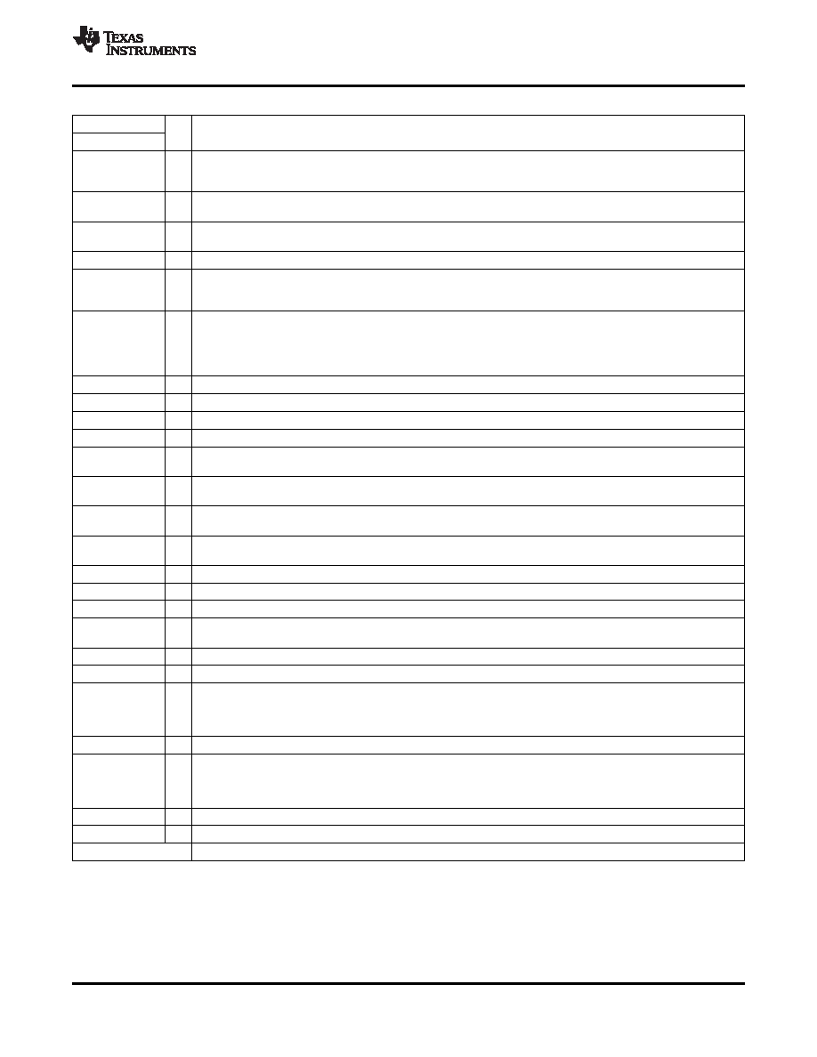
PIN FUNCTIONS
PIN
I/O
DESCRIPTION
NAME
NO.
This is the supply pin of the positive charge pump driver and can be connected to the input supply VIN or the
SUP
8
I
output of the main boost converter VS. This depends mainly on the desired output voltage VGH and numbers of
charge pump stages.
Frequency adjust pin. This pin allows setting the switching frequency with a logic level to 500 kHz = low and
FREQ
12
I
750 kHz = high.
Analog input voltage of the device. This is the input for the analog circuits of the device and should be bypassed
AVIN
22
I
with a 1-
μF ceramic capacitor for good filtering.
VINB
20, 21
I
Power input voltage pin for the buck converter.
This is the enable pin of the buck converter and negative charge pump. When this pin is pulled high, the buck
EN1
16
I
converter starts up, and after a delay time set by DLY1, the negative charge pump comes up. This pin must be
terminated and not be left floating. A logic high enables the device and a logic low shuts down the device.
The boost converter starts only with EN1 = high, after the step-down converter is enabled. EN2 is the enable pin
of the boost converter and positive charge pump. When this pin is pulled high, the boost converter and positive
EN2
9
I
charge pump starts up after the buck converter is within regulation and a delay time set by DLY2 has passed by.
This pin must be terminated and not be left floating. A logic high enables the device and a logic low shuts down
the device.
DRN
11
O
Drive pin of the negative charge pump.
FBN
13
I
Feedback pin of negative charge pump.
REF
24
O
Internal reference output typically 1.213 V. A 220-nF capacitor needs to be connected to this pin.
PGND
6, 7
Power ground
This pin allows setting the soft-start time for the main boost converter VS. Typically a 22-nF capacitor needs to be
SS
28
O
connected to this pin to set the soft-start time.
Connecting a capacitor from this pin to GND allows the setting of the delay time between V(LOGIC) (step-down
DLY1
25
O
converter output high) to VGL during start-up.
Connecting a capacitor from this pin to GND allows the setting of the delay time between V(LOGIC) (step-down
DLY2
26
O
converter output high) to VS boost converter and positive charge-pump VGH during start-up.
This is the compensation pin for the main boost converter. A small capacitor and, if required, a resistor is
COMP
2
connected to this pin.
FBB
15
I
Feedback pin of the buck converter
SWB
18
O
Switch pin of the buck converter
NC
19
Not connected
N-channel MOSFET gate drive voltage for the buck converter. Connect a capacitor from the switch node SWB to
BOOT
17
I
this pin.
FBP
14
I
Feedback pin of positive charge pump.
DRP
10
O
Drive pin of the positive charge pump.
This is the gate drive pin which can be used to control an external MOSFET switch to provide input to output
isolation of VS or VGH. See the circuit diagrams at the end of this data sheet. GD is an open-drain output and is
GD
27
latched low as soon as the boost converter is within 8% of its nominal regulated output voltage. GD goes high
impedance when the EN2 input voltage is cycled low.
GND
23
Analog ground
Output sense pin. The OS pin is connected to the internal rectifier switch and overvoltage protection comparator.
This pin needs to be connected to the output of the boost converter and cannot be connected to any other voltage
OS
3
I
rail. Connect a 470-nF capacitor from OS pin to GND to avoid noise coupling into this pin. The PCB trace of the
OS pin needs to be wide because it conducts high current.
FB
1
I
Feedback of the main boost converter generating Vsource (VS).
SW
4, 5
I
Switch pin of the boost converter generating Vsource (VS).
PowerPAD
The PowerPAD needs to be connected and soldered to power ground (PGND).
Copyright 2006–2009, Texas Instruments Incorporated
7
相關(guān)PDF資料 |
PDF描述 |
|---|---|
| TPS65162RGZR | 4.2 A SWITCHING REGULATOR, 900 kHz SWITCHING FREQ-MAX, PQCC48 |
| TPS65167ARHARG4 | 4.9 A SWITCHING REGULATOR, 900 kHz SWITCHING FREQ-MAX, PQCC40 |
| TPS65167RHAT | 4.9 A SWITCHING REGULATOR, 900 kHz SWITCHING FREQ-MAX, PQCC40 |
| TPS65170RHDT | 4.2 A SWITCHING REGULATOR, 900 kHz SWITCHING FREQ-MAX, PQCC28 |
| TPS65171RHAR | 4 A SWITCHED CAPACITOR REGULATOR, 900 kHz SWITCHING FREQ-MAX, PQCC40 |
相關(guān)代理商/技術(shù)參數(shù) |
參數(shù)描述 |
|---|---|
| TPS65161BPWPR | 功能描述:其他電源管理 Bias supply for TV & Monitor LCD Panel RoHS:否 制造商:Texas Instruments 輸出電壓范圍: 輸出電流:4 mA 輸入電壓范圍:3 V to 3.6 V 輸入電流: 功率耗散: 工作溫度范圍:- 40 C to + 110 C 安裝風(fēng)格:SMD/SMT 封裝 / 箱體:VQFN-48 封裝:Reel |
| TPS65161BPWPRG4 | 功能描述:其他電源管理 Bias supply for TV & Monitor LCD Panel RoHS:否 制造商:Texas Instruments 輸出電壓范圍: 輸出電流:4 mA 輸入電壓范圍:3 V to 3.6 V 輸入電流: 功率耗散: 工作溫度范圍:- 40 C to + 110 C 安裝風(fēng)格:SMD/SMT 封裝 / 箱體:VQFN-48 封裝:Reel |
| TPS65161EVM-194 | 功能描述:電源管理IC開發(fā)工具 PWR SPPLY FOR LCD PANELS RoHS:否 制造商:Maxim Integrated 產(chǎn)品:Evaluation Kits 類型:Battery Management 工具用于評估:MAX17710GB 輸入電壓: 輸出電壓:1.8 V |
| TPS65161PWPR | 功能描述:LCD 驅(qū)動器 12V/2.8A(I/O) 4-CH Multi-Converter RoHS:否 制造商:Maxim Integrated 數(shù)位數(shù)量:4.5 片段數(shù)量:30 最大時鐘頻率:19 KHz 工作電源電壓:3 V to 3.6 V 最大工作溫度:+ 85 C 最小工作溫度:- 20 C 封裝 / 箱體:PDIP-40 封裝:Tube |
| TPS65161PWPRG4 | 功能描述:LCD 驅(qū)動器 12V/2.8A(I/O) 4-CH Multi-Converter RoHS:否 制造商:Maxim Integrated 數(shù)位數(shù)量:4.5 片段數(shù)量:30 最大時鐘頻率:19 KHz 工作電源電壓:3 V to 3.6 V 最大工作溫度:+ 85 C 最小工作溫度:- 20 C 封裝 / 箱體:PDIP-40 封裝:Tube |
發(fā)布緊急采購,3分鐘左右您將得到回復(fù)。