- 您現(xiàn)在的位置:買賣IC網(wǎng) > PDF目錄98300 > TS8388BCF 1-CH 8-BIT PROPRIETARY METHOD ADC, PARALLEL ACCESS, CQFP68 PDF資料下載
參數(shù)資料
| 型號: | TS8388BCF |
| 元件分類: | ADC |
| 英文描述: | 1-CH 8-BIT PROPRIETARY METHOD ADC, PARALLEL ACCESS, CQFP68 |
| 封裝: | CERAMIC, QFP-68 |
| 文件頁數(shù): | 22/44頁 |
| 文件大小: | 850K |
| 代理商: | TS8388BCF |
第1頁第2頁第3頁第4頁第5頁第6頁第7頁第8頁第9頁第10頁第11頁第12頁第13頁第14頁第15頁第16頁第17頁第18頁第19頁第20頁第21頁當前第22頁第23頁第24頁第25頁第26頁第27頁第28頁第29頁第30頁第31頁第32頁第33頁第34頁第35頁第36頁第37頁第38頁第39頁第40頁第41頁第42頁第43頁第44頁
29
Preliminary Beta-Site
Specification
TS8388BF
This is true so long as the out of phase analog input pin VINB is 50 ohms terminated very closely to one of the neighboring shield ground pins (52,
53, 58, 59) which constitute the local ground reference for the inphase analog input pin (VIN).
Thus the differential analog input preamplifier will fully reject the local ground noise ( and any capacitively and inductively coupled noise) as common
mode effects.
In typical single–ended configuration, enter on the (VIN) input pin, with the inverted phase input pin (VINB) grounded through the 50 ohms
termination resistor.
In single–ended input configuration, the in-phase input amplitude is 0.5 Volt peak to peak,centered on 0V. (or -2 dBm into 50 ohms.)
The inverted phase input is at ground potential through the 50 ohms termination resistor.
However, dynamic performances can be somewhat improved by entering either analog or clock inputs in differential mode.
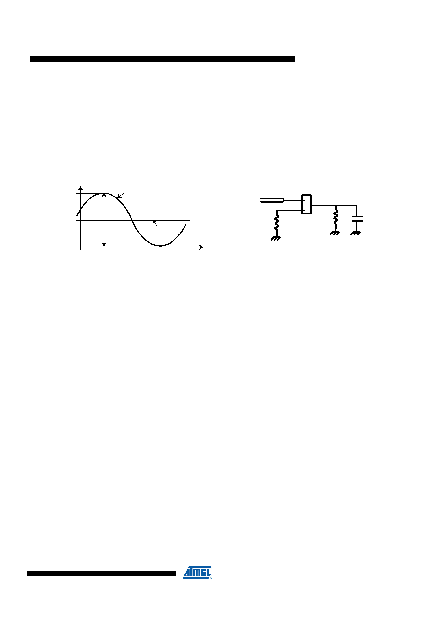
Typical Single ended analog input configuration
VIN or VINB
VIN or VINB double pad (pins 54, 55 or 56, 57)
50
(external)
50
reverse termination
1M
3 pF
-250
250
[mV]
500 mV
Full Scale
analog input
t
VINB
VIN
VINB = 0V
V
IN
= +/- 250 mV
500 mV diff
7.4.
CLOCK INPUTS (CLK) (CLKB)
The TS8388BF can be clocked at full speed without noticeable performance degradation in either differential or single ended configuration.
This is explained by the fact the ADC uses a differential preamplifier stage for the clock buffer, which has been designed in order to be entered either
in differential or single–ended mode.
7.4.1.
SINGLE ENDED CLOCK INPUT (GROUND COMMON MODE)
Although the clock inputs were intended to be driven differentially with nominal -0.8V / -1.8V ECL levels, the TS8388BF clock buffer can manage a
single–ended sinewave clock signal centered around 0 Volt. This is the most convenient clock input configuration as it does not require the use of a
power splitter.
No performance degradation ( e.g. : due to timing jitter) is observed in this particular single–ended configuration up to 1.2GSPS Nyquist conditions (
Fin = 600 MHz ).
This is true so long as the inverted phase clock input pin is 50 ohms terminated very closely to one of the neighbouring shield ground pin, which
constitutes the local Ground reference for the inphase clock input.
Thus the TS8388BF differential clock input buffer will fully reject the local ground noise ( and any capacitively and inductively coupled noise) as
common mode effects.
Moreover, a very low phase noise sinewave generator must be used for enhanced jitter performance.
The typical inphase clock input amplitude is 1 Volt peak to peak, centered on 0 Volt (ground) common mode.
This corresponds to a typical clock input power level of 4 dBm into the 50 ohms termination resistor.
Do not exceed 10 dBm to avoid saturation of the preamplifier input transistors.
The inverted phase clock input is grounded through the 50 ohms termination resistor.
相關(guān)PDF資料 |
PDF描述 |
|---|---|
| TS8388BVF | 1-CH 8-BIT PROPRIETARY METHOD ADC, PARALLEL ACCESS, CQFP68 |
| TS8388BMFB/Q | 1-CH 8-BIT PROPRIETARY METHOD ADC, PARALLEL ACCESS, CQFP68 |
| TS8388BMF | 1-CH 8-BIT PROPRIETARY METHOD ADC, PARALLEL ACCESS, CQFP68 |
| TS8388BCG | 1-CH 8-BIT PROPRIETARY METHOD ADC, PARALLEL ACCESS, CBGA72 |
| TS8388BCG | 1-CH 8-BIT PROPRIETARY METHOD ADC, PARALLEL ACCESS, CBGA72 |
相關(guān)代理商/技術(shù)參數(shù) |
參數(shù)描述 |
|---|---|
| TS8388BCFS | 制造商:e2v technologies 功能描述:ADC 8-BIT 1 GSPS - Trays |
| TS8388BCG | 制造商:未知廠家 制造商全稱:未知廠家 功能描述:A/D CONVERTER |
| TS8388BCGL | 制造商:e2v technologies 功能描述:ADC 8-BIT 1 GSPS - Trays |
| TS8388BCGL (+LID) | 制造商:e2v technologies 功能描述:ADC 8-BIT 1 GSPS - Trays |
| TS8388BMF | 制造商:e2v technologies 功能描述:ADC 8-BIT 1 GSPS - Trays |
發(fā)布緊急采購,3分鐘左右您將得到回復(fù)。