- 您現在的位置:買賣IC網 > PDF目錄98301 > TSA1201IFT (STMICROELECTRONICS) 1-CH 12-BIT PROPRIETARY METHOD ADC, PARALLEL ACCESS, PQFP48 PDF資料下載
參數資料
| 型號: | TSA1201IFT |
| 廠商: | STMICROELECTRONICS |
| 元件分類: | ADC |
| 英文描述: | 1-CH 12-BIT PROPRIETARY METHOD ADC, PARALLEL ACCESS, PQFP48 |
| 封裝: | 7 X 7 MM, PLASTIC, TQFP-48 |
| 文件頁數: | 5/20頁 |
| 文件大小: | 349K |
| 代理商: | TSA1201IFT |
TSA1201
13/20
Slew Rate Control (SRC)
When set to high level (VIH), all digital outputs
currents are limited to a clamp value so that digital
noise power is reduced to its minimum. Rise and
fall times just match 25MHz sampling rate
assuming the load capacitance on each digital
output remains below 10pF.
When set to low level (VIL), the maximum digital
output current increases so that rise and fall times
just match the 50MHz sampling rate assuming the
load capacitance on each digital output remains
below 10pF.
Out of Range (OR)
This function is implemented on the output stage
in order to set up an "Out of Range" flag whenever
the digital data is over the full scale range.
Typically, there is a detection of all the data being
at ’0’ or all the data being at ’1’. This ends up with
an output signal OR which is in low level state
(VOL) when the data stay within the range, or in
high level state (VOH) when the data are out of the
range.
Data Ready (DR)
The Data Ready output is an image of the clock
being synchronized on the output data (D0 to
D11). This is a very helpful signal that simplifies
the
synchronization
of
the
measurement
equipment or the controlling DSP.
As digital output, DR goes into high impedance
state when OEB is asserted to high level as
described in the timing diagram.
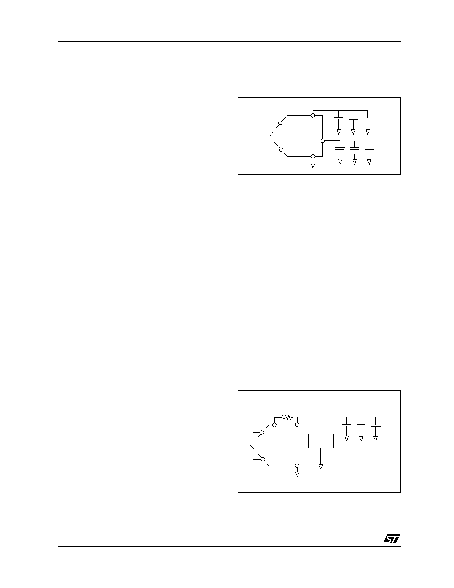
REFERENCES AND COMMON MODE
CONNECTION
It is advised to always connect VREFM externally.
Internal reference and common mode
In the default configuration, the ADC operates with
its own reference and common mode voltages
generated by its internal bandgap. VREFM pin is
connected externally to the Analog Ground while
VREFP (respectively INCM) is set to its internal
voltage of 1.03V (respectively 0.57V). It is
recommended to decouple the VREFP in order to
minimize low and high frequency noise (refer to
Figure 1)
Figure 1 : Internal reference and common mode
setting
External reference and common mode
Each of the voltages VREFM, VREFP and INCM
can be fixed externally to better fit to the
application needs (Refer to table ’OPERATING
CONDITIONS’ page 2 for min/max values).
The VREFP, VREFM voltages set the analog
dynamic at the input of the converter that has a full
scale amplitude of 2*(VREFP-VREFM).
In case of analog dynamic lower than 2Vpp, the
best linearity
and
distortion
performance
is
achieved while increasing the VREFM voltage
instead of lowering the VREFP one.
The INCM is the mid voltage of the analog input
signal.
It is possible to use an external reference voltage
device for specific applications requiring even
better
linearity,
accuracy
or
enhanced
temperature behavior.
Using
the
STMicroelectronics
TS821
or
TS4041-1.2 Vref leads to optimum performances
when configured as shown on Figure 2.
Figure 2 : External reference setting
This
can
be
very
helpful
for
example
for
multichannel application to keep a good matching
among the sampling frequency range.
TSA1201
VIN
VINB
VREFM
1.03V
VREFP
330pF
4.7uF
10nF
INCM
330pF
4.7uF
10nF
0.57V
1k
TSA1201
VIN
VINB
VREFM
VREFP
external
reference
VCCA
330pF
4.7uF
10nF
TS821
TS4041
相關PDF資料 |
PDF描述 |
|---|---|
| TSA1203IFT | 2-CH 12-BIT PROPRIETARY METHOD ADC, PARALLEL ACCESS, QFP48 |
| TSA1203IF | 2-CH 12-BIT PROPRIETARY METHOD ADC, PARALLEL ACCESS, QFP48 |
| TSA1203IFT-E | 2-CH 12-BIT PROPRIETARY METHOD ADC, PARALLEL ACCESS, QFP48 |
| TSA1204IFT-E | 2-CH 12-BIT PROPRIETARY METHOD ADC, PARALLEL ACCESS, PQFP48 |
| TSA1204IFT | 2-CH 12-BIT PROPRIETARY METHOD ADC, PARALLEL ACCESS, PQFP48 |
相關代理商/技術參數 |
參數描述 |
|---|---|
| TSA1203 | 制造商:STMICROELECTRONICS 制造商全稱:STMicroelectronics 功能描述:DUAL-CHANNEL, 12-BIT, 40MSPS, 230mW A/D CONVERTER |
| TSA1203_06 | 制造商:STMICROELECTRONICS 制造商全稱:STMicroelectronics 功能描述:Dual-channel 12-bit 40Msps 215mW A/D converter |
| TSA1203IF | 功能描述:模數轉換器 - ADC Dual Channel 12-Bit RoHS:否 制造商:Texas Instruments 通道數量:2 結構:Sigma-Delta 轉換速率:125 SPs to 8 KSPs 分辨率:24 bit 輸入類型:Differential 信噪比:107 dB 接口類型:SPI 工作電源電壓:1.7 V to 3.6 V, 2.7 V to 5.25 V 最大工作溫度:+ 85 C 安裝風格:SMD/SMT 封裝 / 箱體:VQFN-32 |
| TSA1203IFT | 功能描述:模數轉換器 - ADC Dual Channel 12-Bit RoHS:否 制造商:Texas Instruments 通道數量:2 結構:Sigma-Delta 轉換速率:125 SPs to 8 KSPs 分辨率:24 bit 輸入類型:Differential 信噪比:107 dB 接口類型:SPI 工作電源電壓:1.7 V to 3.6 V, 2.7 V to 5.25 V 最大工作溫度:+ 85 C 安裝風格:SMD/SMT 封裝 / 箱體:VQFN-32 |
| TSA1203IFT-E | 制造商:STMICROELECTRONICS 制造商全稱:STMicroelectronics 功能描述:Dual-channel 12-bit 40Msps 215mW A/D converter |
發布緊急采購,3分鐘左右您將得到回復。