- 您現(xiàn)在的位置:買賣IC網(wǎng) > PDF目錄98303 > TSM115CD (STMICROELECTRONICS) 4-CHANNEL POWER SUPPLY SUPPORT CKT, PDSO20 PDF資料下載
參數(shù)資料
| 型號: | TSM115CD |
| 廠商: | STMICROELECTRONICS |
| 元件分類: | 電源管理 |
| 英文描述: | 4-CHANNEL POWER SUPPLY SUPPORT CKT, PDSO20 |
| 封裝: | PLASTIC, MICRO SO-20 |
| 文件頁數(shù): | 10/17頁 |
| 文件大小: | 219K |
| 代理商: | TSM115CD |
TSM115
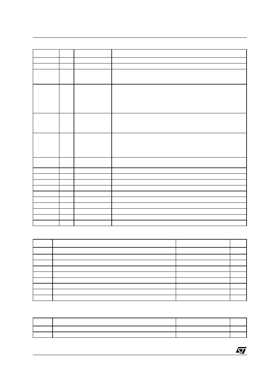
Pin Description
2/17
1
Pin Description
ABSOLUTE MAXIMUM RATINGS
OPERATING CONDITIONS
Name
Pin #
Type
Function
Fault
1
Open collector
Fault output. Output of the over voltage and under voltage comparators.
Gnd
2
Power supply
Signal ground and silicon substrate
PG
4
Open collector
Output of the Tpg comparator. This pin goes low upon an under voltage
condition. Except for the delay set by the Tpg capacitor this pin always
reflects the actual state of the under voltage sensing comparators output.
Tuv/Tpg
5
Timing capacitor
A capacitor from this pin to Gnd provides a delay between outputs rail volt-
age within regulation and PG output going high. Capacitor discharges
whenever Bsense low or Rem high or UVP is detected.
This capacitor will also provide the under voltage blanking function when
the voltage at this pin is larger than the Vref voltage. The under voltage
function resume.
Rem
6
Control Input pin
Pulling this pin high will send the Fault pin high latching off the power sup-
ply, reset the internal latch, discharge the start-up timing capacitors, Tuv
and Tpg capacitors, allowing normal start up of the system. Pulling this pin
low will send the Fault pin low, initiating a normal start up function.
Trem/Tsur
7
Timing capacitor
A capacitor from this pin to Gnd will delay the Fault signal when the Rem
pin is used to shut down the power supply. The PG will signal a power fail-
ure warming immediately, but the Fault pin shut down of the power will be
delayed. This capacitor will also provide the overcurrent blanking function
(surge current).
Bsense
9
Control input pin
Non inverting input to the Bsense voltage sensing comparator. Pulling this
pin lower than 2.5V will cause PG goes low and Tuv goes low.
Vs5
10
Analog input
Over voltage and under voltage detection for +5V rail
Is5
11
Analog Input
5V overcurrent control sense input.
Vs12a
12
Analog input
Over voltage and under voltage detection for +12V rail
Vs12b
13
Analog input
Over voltage and under voltage detection for +12V rail
Vs-12
14
Analog input
Over voltage and under voltage detection for -12V rail.
Is12
15
Analog Input
12V overcurrent control sense input.
Vs3.3
16
Analog input
Over voltage and under voltage detection for 3.3V rail.
Is3.3
17
Analog Input
3.3V overcurrent control sense input.
Rcrnt
19
Analog input
A resistor from this pin to Gnd will provide the internal constant current.
Vcc
20
Power supply
Supply input voltage
Symbol
DC Supply Voltage
Value
Unit
Vcc
DC Supply Voltage 1
-0.3 to 18
V
Vpmax
Terminal voltage Vs3.3, Is3.3, Vs12, Is12, Vs5, Is5
-0.3 to 18
V
Vnmax
Terminal voltage Vs-12
-15 to 5
V
VDBTT
VTpg/Tuv, VTrem/Tsur input voltage
-0.3 to 3.3V
V
VTER
Other terminals
-0.3 to Vcc
V
PT
Power dissipation
1
W
Tstg
Storage temperature
-55 to 150
°C
Tj
Junction temperature
150
°C
ESD
Electrostatic Discharge
2
kV
1) All voltage values, except differential voltage are with respect to network ground terminal.
Symbol
Parameter
Value
Unit
Vcc
DC Supply Conditions
3 to 15
V
Toper
Temperature range
0 to 95
°C
相關(guān)PDF資料 |
PDF描述 |
|---|---|
| TSM121CN | 0.05 A SWITCHING CONTROLLER, 140 kHz SWITCHING FREQ-MAX, PDIP24 |
| TSP2104DBV | SPECIALTY ANALOG CIRCUIT, PDSO5 |
| TPS2104DR | SPECIALTY ANALOG CIRCUIT, PDSO8 |
| TSX83102G0BGS | 1-CH 10-BIT PROPRIETARY METHOD ADC, PARALLEL ACCESS, CBGA152 |
| TUA1030 | 3-BAND, VIDEO TUNER, PDSO24 |
相關(guān)代理商/技術(shù)參數(shù) |
參數(shù)描述 |
|---|---|
| TSM115CN | 制造商:STMICROELECTRONICS 制造商全稱:STMicroelectronics 功能描述:3.3V +5V 【12V Housekeeping IC |
| TSM-116-01-F-DH | 制造商:Samtec Inc 功能描述:CONN UNSHRD HDR HDR 32 POS 2.54MM SLDR RA SMD - Bulk |
| TSM-116-01-F-DH-A | 制造商:Samtec Inc 功能描述:CONN UNSHRD HDR HDR 32 POS 2.54MM SLDR RA SMD - Bulk |
| TSM-116-01-F-DV | 制造商:Samtec Inc 功能描述:.025 SQ. TERMINAL STRIPS - Bulk |
| TSM-116-01-F-DV-A | 制造商:Samtec Inc 功能描述:CONN UNSHRD HDR HDR 32 POS 2.54MM SLDR ST SMD - Bulk |
發(fā)布緊急采購,3分鐘左右您將得到回復(fù)。