- 您現在的位置:買賣IC網 > PDF目錄98307 > TWL1107PW (TEXAS INSTRUMENTS INC) SPECIALTY CONSUMER CIRCUIT, PDSO20 PDF資料下載
參數資料
| 型號: | TWL1107PW |
| 廠商: | TEXAS INSTRUMENTS INC |
| 元件分類: | 消費家電 |
| 英文描述: | SPECIALTY CONSUMER CIRCUIT, PDSO20 |
| 封裝: | PLASTIC, TSSOP-20 |
| 文件頁數: | 15/19頁 |
| 文件大小: | 259K |
| 代理商: | TWL1107PW |
TWL1107
VOICE-BAND AUDIO PROCESSOR (VBAP
)
SLWS119 – JUNE 2001
5
POST OFFICE BOX 655303
DALLAS, TEXAS 75265
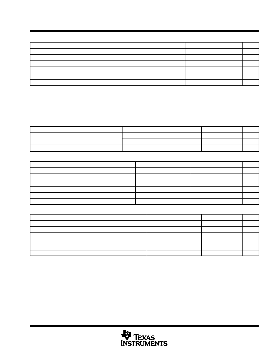
recommended operating conditions (see Note 2)
MIN
NOM
MAX
UNIT
Supply voltage, DVDD, EARVDD
2.7
3.3
V
High-level input voltage, VIH
0.7 x VDD
V
Low-level input voltage, VIL
0.3 x VDD
V
Load impedance between EAROUT+ and EAROUT–, RL
8 to 32
Input voltage, MICIN
0.9 x VDD
V
Operating free-air temperature, TA
– 40
85
_C
NOTES:
1. To avoid possible damage and resulting reliability problems to these CMOS devices, follow the power-up sequence detailed in the
system reliability features paragraph.
2. Voltages are with respect to DVSS and EARVSS.
electrical characteristics over recommended ranges of supply voltage and operating free-air temperature
(unless otherwise noted)
supply current
PARAMETER
TEST CONDITIONS
MIN
TYP
MAX
UNIT
I
Supply current from V
Operating
5
7
mA
IDD
Supply current from VDD
Power down, MCLK not present
10
30
A
tpu
Power-up time from power down
10
ms
digital interface
PARAMETER
TEST CONDITIONS
MIN
TYP
MAX
UNIT
VOH
High-level output voltage, PCMO
IOH = – 3.2 mA,
VDD = 3 V
DVDD – 0.25
V
VOL
Low-level output voltage, PCMO
IOL = 3.2 mA,
VDD = 3 V
0.2
V
IIH
High-level input current, any digital input
VI = 2.2 V to VDD
10
A
IIL
Low-level input current, any digital input
VI = 0 to 0.8 V
10
A
CI
Input capacitance
10
pF
Co
Output capacitance
20
pF
microphone interface
PARAMETER
TEST CONDITIONS
MIN
TYP
MAX
UNIT
VIO
Input offset voltage
See Note 3
– 5
5
mV
IIB
Input bias current
– 250
250
nA
Ci
Input capacitance
5
pF
Vn
Microphone input referred noise, psophometric weighted
MIC Amp 1 gain = 23.5 dB,
See Note 4
2.9
4
Vrms
MICMUTE
– 80
dB
NOTES:
3. Measured while MICIN+ and MICIN– are connected together. Less than 0.5 mV offset results in 0 value code on PCMOUT.
4. Configured as shown in Figure 3.
相關PDF資料 |
PDF描述 |
|---|---|
| TWL1110GQE | SPECIALTY CONSUMER CIRCUIT, PBGA80 |
| TWL1110PBSR | SPECIALTY CONSUMER CIRCUIT, PQFP32 |
| TWL1110GQER | SPECIALTY CONSUMER CIRCUIT, PBGA80 |
| TWL1110PBS | SPECIALTY CONSUMER CIRCUIT, PQFP32 |
| TWL2213CAPFBR | 1-CHANNEL POWER SUPPLY SUPPORT CKT, PQFP48 |
相關代理商/技術參數 |
參數描述 |
|---|---|
| TWL1107PWR | 制造商:Rochester Electronics LLC 功能描述:- Bulk |
| TWL1109 | 制造商:TI 制造商全稱:Texas Instruments 功能描述:VOICE-BAND AUDIO PROCESSOR VBAPE |
| TWL1109PBS | 制造商:TI 制造商全稱:Texas Instruments 功能描述:VOICE-BAND AUDIO PROCESSOR VBAPE |
| TWL1109PBSR | 制造商:未知廠家 制造商全稱:未知廠家 功能描述:PCM CODEC|SINGLE|TQFP|32PIN|PLASTIC |
| TWL1110 | 制造商:TI 制造商全稱:Texas Instruments 功能描述:VOICE-BAND AUDIO PROCESSOR VBAPE |
發布緊急采購,3分鐘左右您將得到回復。