- 您現在的位置:買賣IC網 > PDF目錄382704 > U4285BM-AFSG3 AM / FM - PLL PDF資料下載
參數資料
| 型號: | U4285BM-AFSG3 |
| 英文描述: | AM / FM - PLL |
| 中文描述: | 調幅/調頻-鎖相環 |
| 文件頁數: | 5/10頁 |
| 文件大小: | 138K |
| 代理商: | U4285BM-AFSG3 |
U4285BM
TELEFUNKEN Semiconductors
Rev. A3, 14-May-97
5 (10)
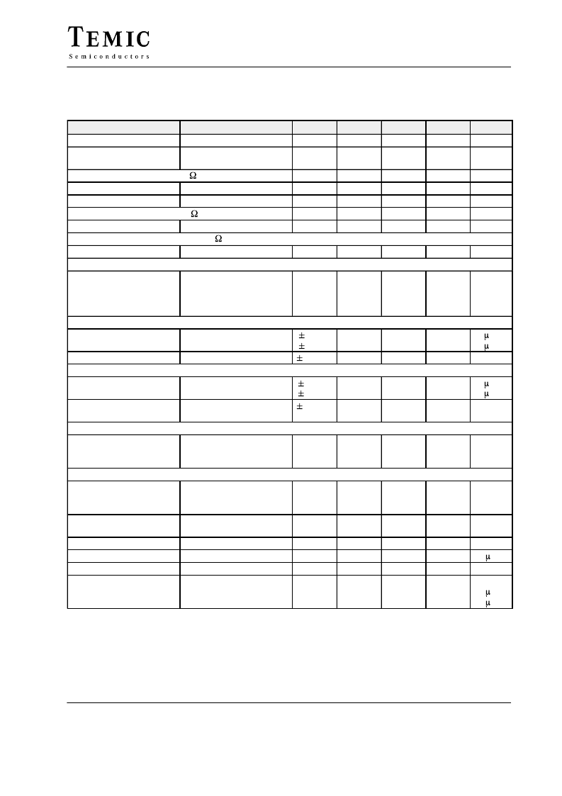
Electrical Characteristics
V
DD
= 5 V, V
A
= 10 V, T
amb
= 25
°
C, unless otherwise specified
Parameters
Test conditions / Pin
Symbol
V
DD
I
DD
Min.
4.5
Typ.
5.0
4.0
4.0
Max.
5.5
7.0
7.0
Unit
V
mA
Supply voltage
Quiescent supply current
Pin 1
Pin 1
AM-mode
FM-mode
FM input sensitivity, R
G
= 50 FMOSC
f
i
= 70 to 120 MHz
f
i
= 160 MHz
AM input sensitivity, R
G
= 50 AMOSC
f
i
= 0.6 to 35 MHz
Oscillator input sensitivity, R
G
= 50 OSCIN
f
i
= 0.1 to 15 MHz
Switching output SWO 1, SWO 2, SWO 3, SWO 4 (open drain)
Output voltage
LOW
Output leakage current
HIGH
V5, V6, V7, V8 = 10 V
Phase detector PDFM
Output current 1
Output current 2
Leakage current
Phase detector PDAM
Output current 1
Output current 2
Leakage current
Pin 9
Pin 9
V
SFM
V
SFM
40
150
mV
rms
mV
rms
Pin 11
V
SAM
40
mV
rms
Pin 18
V
SOSC
100
mV
rms
Pins 5, 6, 7 and 8
I
L
= 1 mA
Pins 5, 6, 7 and 8
V
SWOL
I
OHL
100
400
100
mV
nA
Pin 13
Pin 13
Pin 13
I
PDFM
I
PDFM
I
PDFML
1600
400
2000
500
2400
600
20
A
A
nA
Pin 14
Pin 14
Pin 14
I
PDAM
I
PDAM
I
PDAM-
L
160
40
200
50
240
60
20
A
A
nA
Analogue output PDFMO, PDAMO
Saturation voltage
LOW
HIGH
I
2
C bus SCL, SDA, AS
Input voltage
HIGH
LOW
Output voltage
Acknowledge LOW
Clock frequency
Rise time SDA, SCL
Fall time SDA, SCL
Period of SCL
HIGH
LOW
Pins 12 and 15
I = 15 mA
V
satL
V
satH
9.5
200
9.95
400
mV
V
Pins 2, 3 and 4
V
iBUS
3.0
0
V
DD
1.5
V
V
Pin 3
I
SDA
= 3 mA
V
O
f
SCL
t
r
t
f
0.4
100
1
300
V
Pin 2
kHz
Pins 2 and 3
Pins 2 and 3
s
ns
Pin 2
HIGH
LOW
t
H
t
L
4.0
4.7
s
s
相關PDF資料 |
PDF描述 |
|---|---|
| U4285BM | AM / FM - PLL |
| U4285BM-BFP | Consumer IC |
| U4285BM-BFS | Consumer IC |
| U4286BM-BFP | AM / FM-PLL |
| U4286BM-BFPG3 | AM / FM-PLL |
相關代理商/技術參數 |
參數描述 |
|---|---|
| U4285BM-BFP | 制造商:未知廠家 制造商全稱:未知廠家 功能描述:Consumer IC |
| U4285BM-BFS | 制造商:未知廠家 制造商全稱:未知廠家 功能描述:Consumer IC |
| U4285BM-MFS | 功能描述:IC PLL AM/FM W/4 SWITCHES 20SSOP RoHS:否 類別:RF/IF 和 RFID >> RF 其它 IC 和模塊 系列:- 標準包裝:100 系列:* |
| U4285BM-MFSG3 | 功能描述:IC PLL AM/FM W/4 SWITCHES 20SSOP RoHS:是 類別:RF/IF 和 RFID >> RF 其它 IC 和模塊 系列:- 標準包裝:100 系列:* |
| U4286BM | 制造商:TEMIC 制造商全稱:TEMIC Semiconductors 功能描述:AM / FM-PLL |
發布緊急采購,3分鐘左右您將得到回復。