- 您現在的位置:買賣IC網 > PDF目錄382705 > U4313B-AFL Low-Current Superhet Remote Control Receiver PDF資料下載
參數資料
| 型號: | U4313B-AFL |
| 英文描述: | Low-Current Superhet Remote Control Receiver |
| 中文描述: | 低電流超外差遙控接收器 |
| 文件頁數: | 3/14頁 |
| 文件大小: | 167K |
| 代理商: | U4313B-AFL |
TELEFUNKEN Semiconductors
U4313B
Rev. A1: 23.06.1995
3 (14)
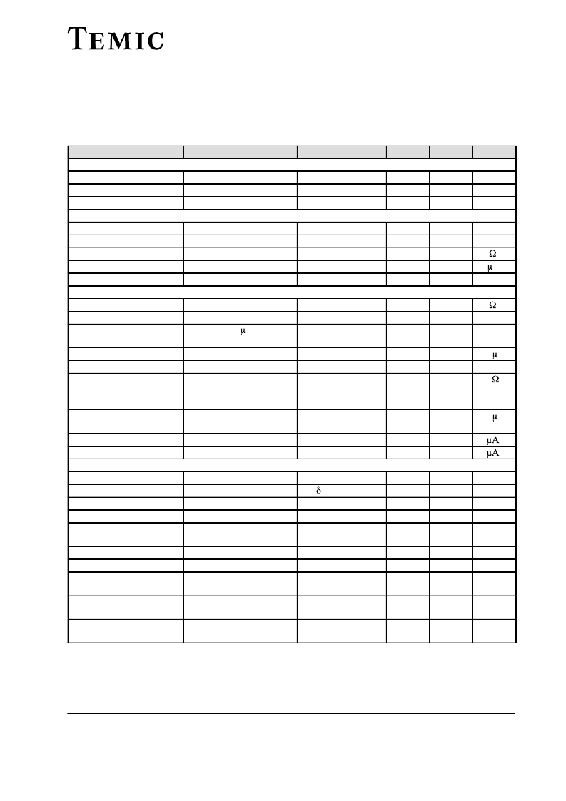
Electrical Characteristics
V
S
= 5 V, T
amb
= 25
°
C, f
in
= 10.7 MHz; FM part: f
mod
= 1 kHz, f
dev
= 22.5 kHz; AM part:, f
mod
= 1 kHz, m = 100%
unless otherwise specified
Parameters
Test Conditions / Pins
Symbol
Min.
Typ.
Max.
Unit
Characteristics
Supply voltage range
Quiescent supply current
Active supply current
Bandgap
Regulated voltage
Output current
Source resistance
External capacitor
Power supply suppression
IF amplifier
Input resistance
Input capacitance
Typical internal 3 dB
frequency
–3 dB limiting point
Recovered data voltage
FM detector output
resistance
AM rejection ratio
Maximum AM input
voltage
AM quiescent current
Maximum AM current
Operational amplifier
Gain bandwidth product
Excess phase
Open loop gain
Output voltage range
Common mode input
voltage
Input offset voltage
Maximum output current
Common mode rejection
ratio
Total harmonic distortion
Pin 15
Pin 15
Pin 15
V
S
I
q
I
act
3
12
1.3
3.6
V
1
mA
mA
2.8
Pin 13
Pin 13
Pin 13
Pin 13
Pin 13
V
ref
I
ref
R
Ref
C
ref
psrr
2.3
2.4
2.5
5
5
V
mA
2.3
10
F
f = 50 Hz
60
dB
Pin 9
Pin 9
R
in
C
in
f
3dB
180
330
5
520
pF
MHz
IF level 70 dB V
Pins 9 and 14
Pin 9
Pin 14
Pin 14
8
12
V
FM3dB
V
FMout
R
FMout
30
130
50
dB V
mV
k
50
230
m = 30%
Pins 9 and 14
Pin 9
AM
rr
V
AMmax
25
90
dB
dB V
Pin 8
Pin 8
I
AMout
I
AMoutmax
10
22
100
37
Pins 1, 2 and 16
Pins 1, 2 and 16
Pins 1, 2 and 16
Pin 2
Pins 1 and 16
f
t
3
4
80
70
1.55
6.5
MHz
degree
dB
V
V
g
0
50
95
V
out
V
in
0.7
1.7
Pins 1 and 16
Pin 2
Pins 1 and 16
V
os
I
out
cmrr
–2.5
0
+2.5
5
mV
mA
dB
65
85
V
in
< 300 mV, f = 33 kHz,
unity gain circuit Pin 2
f = 50 Hz
thd
1
3
%
Power supply rejection
ratio
Pin 2
psrr
65
85
dB
相關PDF資料 |
PDF描述 |
|---|---|
| U4313B | Low-Current Superhet Remote Control Receiver |
| U4314B | Logarithmic AM Demodulator/RSSI |
| U4314B-AFP | Logarithmic AM Demodulator/RSSI |
| U4459B | IF Amplifier for Cable DVB Processing |
| U4460BG-D | Rail to rail micropower BiCMOS comparators |
相關代理商/技術參數 |
參數描述 |
|---|---|
| U4314 | 制造商:APEM 功能描述: |
| U4314B | 制造商:TEMIC 制造商全稱:TEMIC Semiconductors 功能描述:Logarithmic AM Demodulator/RSSI |
| U4314B-AFP | 制造商:TEMIC 制造商全稱:TEMIC Semiconductors 功能描述:Logarithmic AM Demodulator/RSSI |
| U4316 | 功能描述:開關配件 PushButton Cap Red Rnd,Concave RoHS:否 制造商:C&K Components 類型:Cap 用于:Pushbutton Switches 設計目的: |
| U4317/1 | 制造商:APEM 功能描述: |
發布緊急采購,3分鐘左右您將得到回復。