- 您現在的位置:買賣IC網 > PDF目錄382706 > U6101B IF System and I/Q Demodulator for Digital Satellite TV Transmissions PDF資料下載
參數資料
| 型號: | U6101B |
| 英文描述: | IF System and I/Q Demodulator for Digital Satellite TV Transmissions |
| 中文描述: | 如果系統和I / Q數字衛星電視信號解調器 |
| 文件頁數: | 5/7頁 |
| 文件大小: | 249K |
| 代理商: | U6101B |
U6101B
Preliminary Information
TELEFUNKEN Semiconductors
Rev. A1, 14-May-97
5 (7)
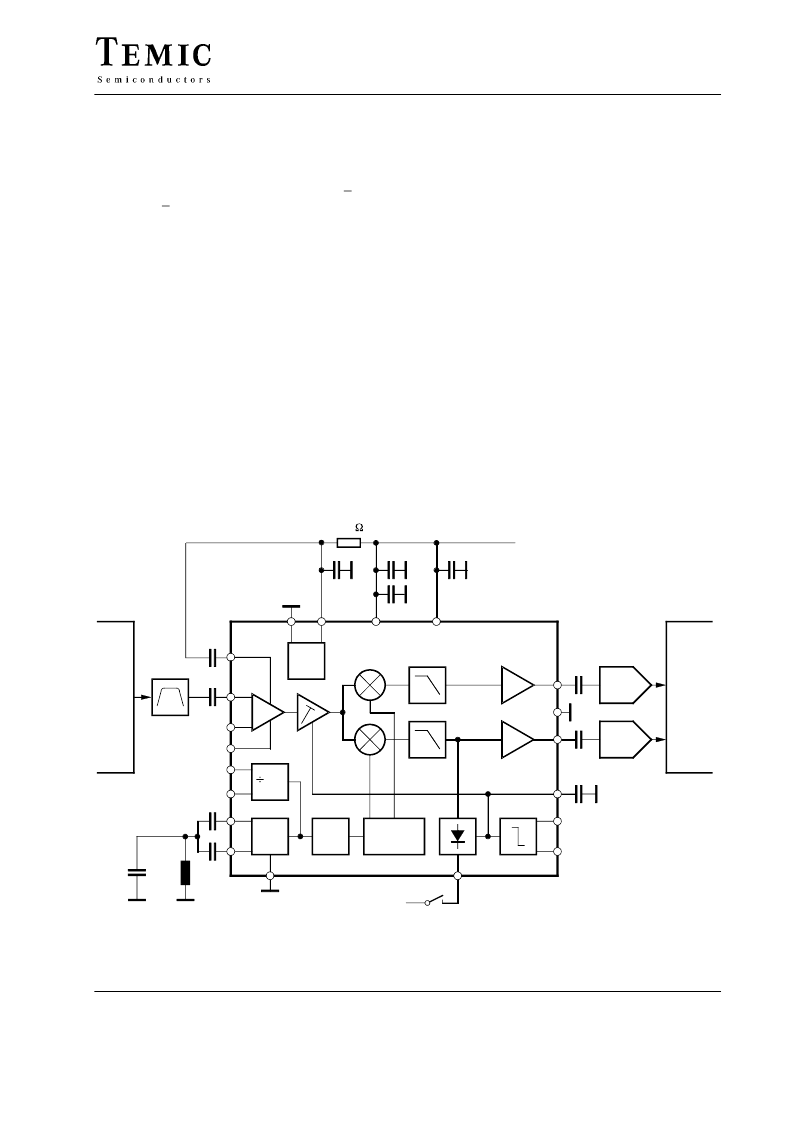
Functional Description
The input signal is via two single ended constant gain
amplifiers with selectable inputs connected to a gain
controlled amplifier. The differential output signal
remains of constant amplitude to provide
splitting up
optimised dynamic operation points for a
pair of identical mixers. The mixer stages are driven by
two orthogonal oscillator signals, to generate the I- and Q-
components.
behind
The oscillator operates at IF-frequency. Therefore control
by an on the shelf SAW resonator is possible. Using the
internal 1/32 frequency divider circuit a VCO carrier
recovery loop can be closed via the base band decoding
system.
Excellent accuracy of 0
°
/90
°
phase shifting between the
demodulator switching carriers is provided by a TEMIC
patented phase correction circuit, which operates in a
wide input frequency range.
Two matched amplifiers with second order lowpass
characteristic to suppress oscillator spurious ensure small
gain and phase errors between both channels and mini-
mize tilt. The output stages may drive complex loads up
to 220
in series to 2.2 k
and 50 pF in a frequency
range up to 40 MHz.
To avoid fast system lock in time and driving the A/D
converters with defined output levels, in one channel the
output signal will be peak-level detected and in an
internally loop level controlled. So the output signal
amplitudes
are
independent
characteristic of the QPSK modulation. The output level
can be set via an external potentiometer (or at two fixed
levels by pin programming) according the actual
application. External loop control by a channel decoder
generated AGC signal is provided.
of
frequency
and
The DC-component of the AGC loop affects the IF input
level. This signal is internally compared with a adjustable
threshold and generates a tuner AGC signal.
Small tolerances based on high DC operation point
stability and good spurious signal suppression are
performed by an internal reference voltage source.
Basic Application Circuit
32
Bias
circuit
f
→
2f
VCO
Divider +
90
°
control
Tuner
A / D
Channel
decoder
A / D
12608
19
1
20
10 nF
1 nF
4.7
100 pF
12
10 nF
+5 V
10 pF
10 pF
3
2
4
9
100 pF
100 pF
17
18
14
15
22 nH
2.2 pF
SW 2
16
13
+5 V
11
10
7
100 nF
100 nF
8
100 nF
6
5
Figure 3. Internal AGC loop, output level optional changeable 0.6 Vpp to 1 Vpp
by control voltage at Pin 13, VCO carrier recovery
相關PDF資料 |
PDF描述 |
|---|---|
| U6102B-AFSG3 | Low power quad operational amplifiers |
| U6207B | 1.3 GHz PLL with I2C Bus for TV Tuner |
| U6207B-FPG3 | 1.3 GHz PLL with I2C Bus for TV Tuner |
| U6209B-FFP | Low power quad operational amplifier |
| U6209B | 1.3 GHz PLL for TV- and VCR- Tuner |
相關代理商/技術參數 |
參數描述 |
|---|---|
| U6101B-AFSG3 | 制造商:未知廠家 制造商全稱:未知廠家 功能描述:TV Video Receiver Circuit |
| U6102B-AFSG3 | 制造商:未知廠家 制造商全稱:未知廠家 功能描述:TV Video Receiver Circuit |
| U6105 | 功能描述:開關配件 Accessories RoHS:否 制造商:C&K Components 類型:Cap 用于:Pushbutton Switches 設計目的: |
| U6106 | 功能描述:開關配件 Rotary Switch RoHS:否 制造商:C&K Components 類型:Cap 用于:Pushbutton Switches 設計目的: |
| U6107 | 功能描述:開關配件 Rotary Switch RoHS:否 制造商:C&K Components 類型:Cap 用于:Pushbutton Switches 設計目的: |
發布緊急采購,3分鐘左右您將得到回復。