- 您現在的位置:買賣IC網 > PDF目錄382706 > U6225B-FPG3 2.9 GHz PLL for SAT TV Receiver with Universal Bus PDF資料下載
參數資料
| 型號: | U6225B-FPG3 |
| 英文描述: | 2.9 GHz PLL for SAT TV Receiver with Universal Bus |
| 中文描述: | 2.9 GHz的鎖相環通用總線的衛星電視接收器 |
| 文件頁數: | 6/12頁 |
| 文件大小: | 166K |
| 代理商: | U6225B-FPG3 |
TELEFUNKEN Semiconductors
U6225B
Rev. A1: 25.10.1995
6 (12)
riod, and then also during the acknowledge periods, when
additional data bytes are programmed. After the address
transmission (first byte), data bytes can be sent to the de-
vice. There are four data bytes requested to fully program
the device. The table ‘I
2
C-Bus Pulse Diagram’ shows
some possible data transfer examples.
Programmable divider bytes PDB1 and PDB2 are stored
in a 15 bit latch and are controlling the division ratio of
the 15 bit programmable divider. The control Byte CB1
allows to control the following special functions:
5I-bit switches between low and high charge pump
current
T1-bit enables divider test mode when it is set to
logic 1
T0-bit allows to disable the charge pump when it is set
to logic 1
OS-bit disable the charge pump drive amplifier output
when it is set to logic 1.
Only in I
2
C bus mode the charge pump current can be con-
trolled. In 3-wire-bus mode there is always the high
charge pump current active. The OS-bit function disables
the complete PLL function. This allows the tuner align-
ment by suppling the tuning voltage directly through the
30 V supply voltage of the tuner.
The control byte CB2 programs the switching outputs SW
1, 4, 5, 6, 7; a logic 0 for high impedance output (off) and
a logic 1 for low impedance output (on).
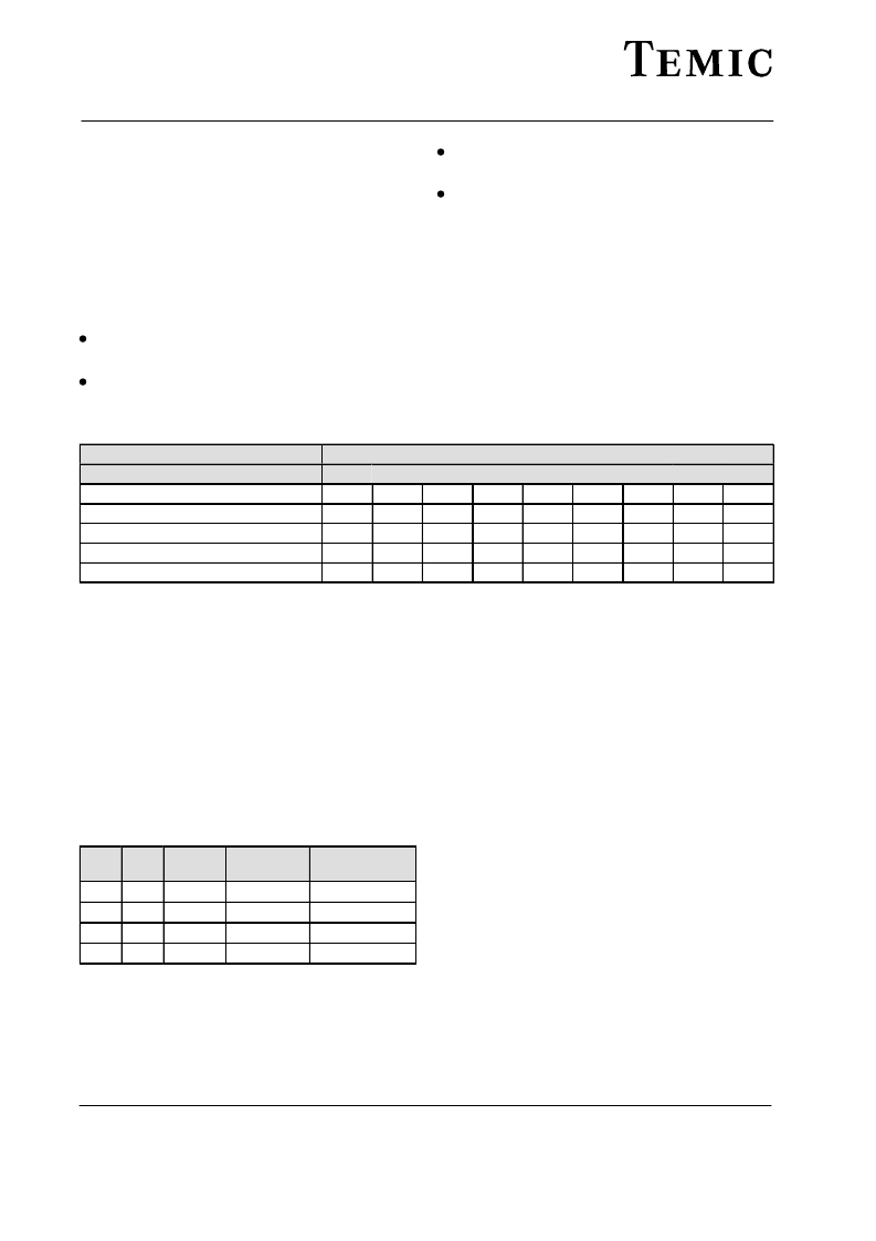
Description
I
2
C Bus Data Format
MSB
1
0
n7
1
SW7
LSB
0
n8
n0
OS
X
Address byte
Progr. divider byte 1
Progr. divider byte 2
Control byte 1
Control byte 2
1
0
0
0
AS1
n10
n2
X
X
AS2
n9
n1
X
SW1
A
A
A
A
A
n14
n6
5I
SW6
n13
n5
T1
SW5
n12
n4
T0
SW4
n11
n3
X
X
A = Acknowledge; X = not used; Unused bits of controlbyte 2 should be 0 for lowest power consumption
n0 ... n14
T0, T1
Scaling factor (SF)
Testmode selection
SF = 16384*n14+8192*n13+ ... +2*n1 + n0
T1 = 1: divider test mode on
T1 = 0: divider test mode off
T0 = 1: charge pump disable
T0 = 0: charge pump enable
SW1, SW4, SW5, SW6, SW7 = 1: open collector active
5I = 1: high current
5I = 0: low current
OS = 1: varicap driver disable
OS = 0: varicap drive enable
SW1, 4, 5, 6, 7
5I
Switching outputs
Charge pump current switch
OS
Output switch
AS1, AS2
Address selection pin 10
AS1
AS2
Address
Dec. Value
Voltage at pin
10
open
0 to 10% Vs
40 to 60% Vs
90 to 100% Vs
0
0
1
1
1
0
0
1
1
2
3
4
194
192
196
198
相關PDF資料 |
PDF描述 |
|---|---|
| U6229B | Low power dual operational amplifier |
| U6239B-AFSG3 | Low power dual operational amplifier |
| U6239B-CFPG3 | Analog Phase-Locked Loop |
| U6262B | Low power dual operational amplifier |
| U6264ASA07 | x8 SRAM |
相關代理商/技術參數 |
參數描述 |
|---|---|
| U6229B | 制造商:TEMIC 制造商全稱:TEMIC Semiconductors 功能描述:DC/DC Converter - Power Supply 28 V |
| U6239B | 制造商:TEMIC 制造商全稱:TEMIC Semiconductors 功能描述:2.9 GHz PLL for SAT TV Tuner with UNi-Bus |
| U6239B-AFPG3 | 制造商:TEMIC 制造商全稱:TEMIC Semiconductors 功能描述:2.9 GHz PLL for SAT TV Tuner with UNi-Bus |
| U6239B-AFSG3 | 制造商:未知廠家 制造商全稱:未知廠家 功能描述:Analog IC |
| U6239B-CFPG3 | 制造商:未知廠家 制造商全稱:未知廠家 功能描述:Analog Phase-Locked Loop |
發布緊急采購,3分鐘左右您將得到回復。