- 您現在的位置:買賣IC網 > PDF目錄382718 > UC2832-EP Military Enhanced Plastic Precision Low Dropout Linear Controllers PDF資料下載
參數資料
| 型號: | UC2832-EP |
| 英文描述: | Military Enhanced Plastic Precision Low Dropout Linear Controllers |
| 中文描述: | 軍事增強塑料精密低壓差線性控制器 |
| 文件頁數: | 3/11頁 |
| 文件大小: | 377K |
| 代理商: | UC2832-EP |
UC2832-EP
PRECISION LOW DROPOUT LINEAR CONTROLLER
SGLS147A
–
JANUARY 2003
–
REVISED MARCH 2003
3
POST OFFICE BOX 655303
DALLAS, TEXAS 75265
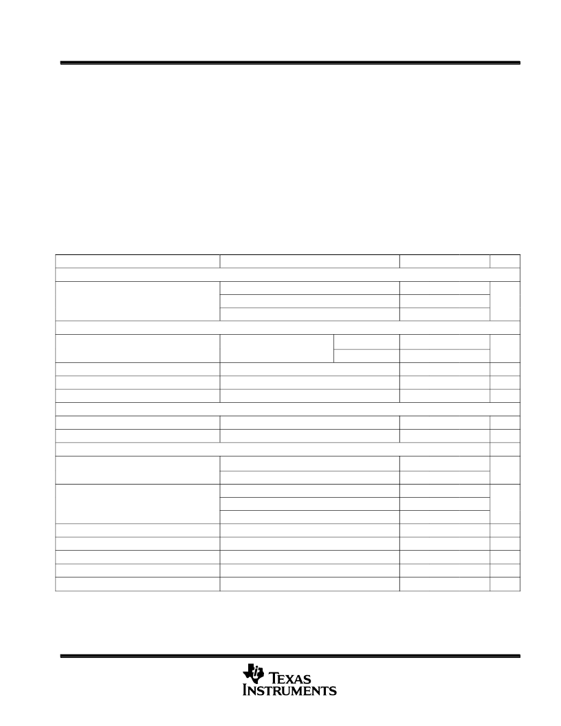
absolute maximum ratings over operating free-air temperature range (unless otherwise noted)
V
IN
supply voltage
. . . . . . . . . . . . . . . . . . . . . . . . . . . . . . . . . . . . . . . . . . . . . . . . . . . . . . . . . . . . . . . . . . . . . . . . .
Driver output current (sink or source), I
O
. . . . . . . . . . . . . . . . . . . . . . . . . . . . . . . . . . . . . . . . . . . . . . . . . .
Driver sink to source voltage
. . . . . . . . . . . . . . . . . . . . . . . . . . . . . . . . . . . . . . . . . . . . . . . . . . . . . . . . . . . . . . . .
TRC pin voltage
. . . . . . . . . . . . . . . . . . . . . . . . . . . . . . . . . . . . . . . . . . . . . . . . . . . . . . . . . . . . . . . . . .
Other input voltages
. . . . . . . . . . . . . . . . . . . . . . . . . . . . . . . . . . . . . . . . . . . . . . . . . . . . . . .
Operating jucntion temperature range, T
J
. . . . . . . . . . . . . . . . . . . . . . . . . . . . . . . . . . . . . . . . . . . .
Storage temperature range, T
stg
. . . . . . . . . . . . . . . . . . . . . . . . . . . . . . . . . . . . . . . . . . . . . . . . . . . .
Lead temperature soldering 1,6 mm (1/16 inch) from case for 10 seconds
40 V
450 mA
40 V
–
0.3 V to 3.2 V
–
0.3 V to supply voltage
–
55 C to 150 C
–
65 C to 150 C
. . . . . . . . . . . . . . . . . . . . . . .
300 C
Stresses beyond those listed under
“
absolute maximum ratings
”
may cause permanent damage to the device. These are stress ratings only, and
functional operation of the device at these or any other conditions beyond those indicated under
“
recommended operating conditions
”
is not
implied. Exposure to absolute-maximum-rated conditions for extended periods may affect device reliability.
Unless otherwise indicated, voltages are reference to ground and currents are positive into and negative out of the specified terminals.
electrical characteristics,
T
A
=
–
40 C to 105 C for the UC2832T-EP, +V
IN
= 15 V, Driver sink = +V
IN
,
C/S(+) voltage = +V
IN
, and T
A
= T
J
(unless otherwise stated)
PARAMETER
TEST CONDITIONS
MIN
TYP
MAX
UNITS
Input Supply
+VIN = 6 V
+VIN = 36 V
Logic Disable = 2 V
6.5
10
Supply current
9.5
15
mA
3.3
10
Reference Section
Output voltage
IDRIVER= 10 mA
IDRIVER = 10 mA
TJ = 25 C
TJ = Full range
1.98
2
2.02
V
1.96
2
2.04
Load regulation voltage
IOUT = 0 to 10 mA
+VIN = 4.5 V to 36 V,
–
10
–
5
10
mV
Line regulation
IDRIVER = 10 mA
0.033
0.5
mV/V
Under-voltage lockout threshold
3.6
4.5
V
Logic Disable Input
Threshold voltage
1.3
1.4
1.5
V
Input bias current
Logic Disable = 0 V
–
5
–
1
0.1
μ
A
Current Sense Section
Comparator offset
TJ = 25 C
TJ = Full range
VADJ = Open
VADJ = 1 V
VADJ = 0 V
VCM = +VIN
VCM = +VIN
VCM = 4.1 V to +VIN + 0.3 V
ICOMP =
100
μ
A
VADJ = 0 V
95
100
105
mV
93
100
107
110
135
170
Amplifier offset
Am lifier offset
180
235
290
mV
250
305
360
Input bias current
65
100
135
μ
A
Input offset current
–
10
10
μ
A
Amplifier CMRR
80
dB
Transconductance
65
ms
VADJ input current
–
10
–
1
μ
A
相關PDF資料 |
PDF描述 |
|---|---|
| UC2834L | DOUBLE CHANNEL HIGH SIDE SOLID STATE RELAY |
| UC2836N | Quad channel high side driver with analog current sense for automotive applications |
| UC2836DW | Positive Adjustable Voltage Regulator |
| UC2836DWTR | QUAD CHANNEL HIGH SIDE DRIVER |
| UC2836J | QUAD CHANNEL HIGH SIDE DRIVER |
相關代理商/技術參數 |
參數描述 |
|---|---|
| UC2832J | 制造商:Texas Instruments 功能描述: |
| UC2832L | 制造商:未知廠家 制造商全稱:未知廠家 功能描述:Positive Adjustable Voltage Regulator |
| UC2832N | 功能描述:低壓差控制器 - LDO Precision LDO Linear RoHS:否 制造商:Micrel 最大輸入電壓:5.5 V 輸出電壓:Adjustable 輸出電流:10 mA 負載調節: 輸出類型:Adjustable, Fixed 輸出端數量:1 最大工作溫度:+ 125 C 安裝風格:SMD/SMT 封裝 / 箱體:SOT-23-6 |
| UC2832NG4 | 功能描述:低壓差控制器 - LDO Precision LDO Linear RoHS:否 制造商:Micrel 最大輸入電壓:5.5 V 輸出電壓:Adjustable 輸出電流:10 mA 負載調節: 輸出類型:Adjustable, Fixed 輸出端數量:1 最大工作溫度:+ 125 C 安裝風格:SMD/SMT 封裝 / 箱體:SOT-23-6 |
| UC2832Q | 制造商:未知廠家 制造商全稱:未知廠家 功能描述:Positive Adjustable Voltage Regulator |
發布緊急采購,3分鐘左右您將得到回復。