- 您現(xiàn)在的位置:買賣IC網(wǎng) > PDF目錄383968 > UD61464DC07 AC LINE SWITCH PDF資料下載
參數(shù)資料
| 型號: | UD61464DC07 |
| 英文描述: | AC LINE SWITCH |
| 中文描述: | x4快速頁面模式的DRAM |
| 文件頁數(shù): | 1/14頁 |
| 文件大小: | 175K |
| 代理商: | UD61464DC07 |
December 12, 1997
1
Maintenance only
UD61464
64K x 4 DRAM
Features
p
Dynamic random access memory
65536 x 4 bits manufactured
using a CMOS technology
RAS access times 70 ns/80 ns
TTL-compatible
Three-state outputs bidirectional
256 refresh cycles
4 ms refresh cycle time
FAST PAGE MODE
Operating modes: Read, Write,
Read - Write,
RAS only Refresh,
Hidden Refresh with address
transfer
Low power dissipation
Power supply voltage 5 V
Package PDIP18 (300 mil)
Operating temperature range
0 to 70 °C
Quality assessment according to
CECC 90000, CECC 90100 and
CECC 90112
p
p
p
p
p
p
p
p
p
p
p
Description
Addressing
The UD61464 is a dynamic random
access memory organized 65536
words by 4 bits.
FPM facilitates faster data operation
with predefined row address. Via 8
address inputs the 16 address bits
are transmitted into the internal
address memories in a time-multi-
plex operation. The falling RAS-
edge takes over the row address.
After the row address hold time the
column address can be applied. The
bit pattern that is available at the
address outputs during the set-up
time and after the falling edge of
CAS is interpreted as row address.
During Write the column address is
taken over with the falling edge of
the control signal CAS, or W, whi-
chever becomes active as the last.
The selection of one or more
memory circuits can be made via the
RAS input.
Read-Write-Control
The choice between Read or Write
cycle is made at the W input. HIGH
at the W input causes a Read cycle,
meanwhile LOW leads to a Write
cycle.
Both CAS-controlled and W-control-
led Write cycles are possible with
activated RAS signal.
Data Output Control
The usual state of the data output is
the High-Z state. Whenever CAS is
inactive (HIGH), Q will float (High-Z).
Thus, CAS functions as data output
control.
After access time, in case of a Read
cycle, the output is activated, and it
contains the logic 0“ or 1“.
If the memory cycle is a Read,
Read-Write or a Write cycle (W-con-
trolled), Q changes from High-Z
state to the active state (0“ or 1“).
After access time, the contents of
the selected cell will be available,
with the exception of the Write cycle.
The output remains active until CAS
becomes inactive, irrespective of
RAS becoming inactive or not. The
memory cycle being a Write cycle
(CAS-controlled), the data output
keeps its High-Z state throughout
the whole cycle. This configuration
makes Q fully controllable by the
user merely through the timing of W.
Through storaging the data on out-
put, they remain valid from the end
of access time until the start of
another cycle.
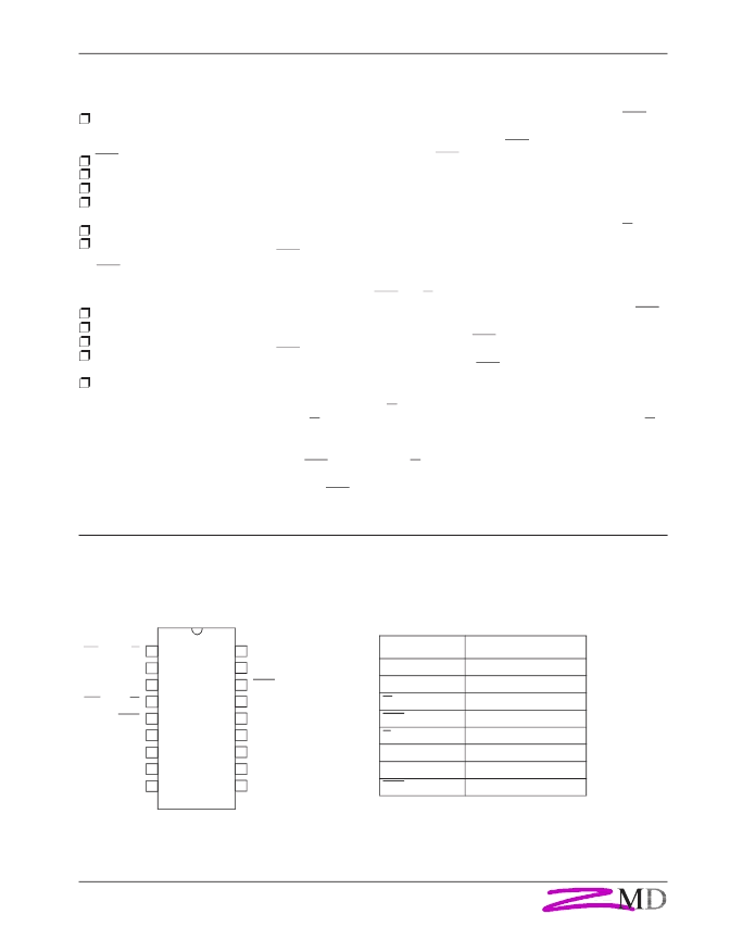
Pin Configuration
1
2
3
G
VSS
DQ3
CAS
18
17
16
DQ0
DQ1
4
5
6
7
8
9
W
DQ2
A6
A3
A4
A5
A7
15
14
13
12
11
10
RAS
A0
A2
A1
VCC
(OE)
(WE)
Pin Description
Signal Name
Signal Description
A0 - A7
DQ0 - DQ3
Address Inputs
Data In/Out
Read, Write Control
Row Address Strobe
Output Enable
Power Supply Voltage
Ground
Column Address Strobe
W
RAS
G
VCC
VSS
CAS
Top View
PDIP
相關(guān)PDF資料 |
PDF描述 |
|---|---|
| UD61464DC08 | AC LINE SWITCH |
| UD61466DC07 | AC LINE SWITCH |
| UD61466DC08 | THREE LINES AC SWITCH ARRAY |
| UDN7180A | High temperature 10 A Triacs |
| UDS3611H883 | 5.0 V and 3.3/3.0 V secure serial RTC and NVRAM supervisor with tamper detection and 128 bytes of clearable NVRAM |
相關(guān)代理商/技術(shù)參數(shù) |
參數(shù)描述 |
|---|---|
| UD61464DC08 | 制造商:未知廠家 制造商全稱:未知廠家 功能描述:x4 Fast Page Mode DRAM |
| UD61466 | 制造商:ZMD 制造商全稱:Zentrum Mikroelektronik Dresden AG 功能描述:64K x 4 DRAM |
| UD61466DC07 | 制造商:ZMD 制造商全稱:Zentrum Mikroelektronik Dresden AG 功能描述:64K x 4 DRAM |
| UD61466DC08 | 制造商:ZMD 制造商全稱:Zentrum Mikroelektronik Dresden AG 功能描述:64K x 4 DRAM |
| UD-6-50N-302 | 制造商:ITT Interconnect Solutions 功能描述:UD-6-50N-302 - Bulk |
發(fā)布緊急采購,3分鐘左右您將得到回復(fù)。