- 您現在的位置:買賣IC網 > PDF目錄363918 > WFW9N90 (Wisdom Semiconductor Inc.) N-Channel MOSFET PDF資料下載
參數資料
| 型號: | WFW9N90 |
| 廠商: | Wisdom Semiconductor Inc. |
| 英文描述: | N-Channel MOSFET |
| 中文描述: | N溝道MOSFET |
| 文件頁數: | 1/2頁 |
| 文件大小: | 115K |
| 代理商: | WFW9N90 |
●
●
●
▲
{
{
{
Absolute Maximum Ratings
Symbol
Parameter
Value
Units
V
DSS
Drain to Source Voltage
900
V
I
D
Continuous Drain Current(@T
C
= 25
°C)
9.0
A
Continuous Drain Current(@T
C
= 100
°C)
5.7
A
I
DM
Drain Current Pulsed
(Note 1)
36.0
±
30
A
V
GS
Gate to Source Voltage
V
E
AS
E
AR
dv/dt
Single Pulsed Avalanche Energy
(Note 2)
986
mJ
Repetitive Avalanche Energy
(Note 1)
26
mJ
Peak Diode Recovery dv/dt
(Note 3)
4.0
V/ns
P
D
Total Power Dissipation(@T
C
= 25 °C)
260
W
Derating Factor above 25 °C
2.08
W/°C
T
STG,
T
J
Operating Junction Temperature & Storage Temperature
- 55 ~ 150
°C
T
L
Maximum Lead Temperature for soldering purpose,
1/8 from Case for 5 seconds.
300
°C
Thermal Characteristics
Symbol
Parameter
Value
Typ.
Units
Min.
Max.
R
θ
JC
R
θ
CS
R
θ
JA
Thermal Resistance, Junction-to-Case
-
-
0.48
°C/W
Thermal Resistance, Case to Sink
-
0.24
-
°C/W
Thermal Resistance, Junction-to-Ambient
-
-
40
°C/W
WFW9N90
1/2
Features
■
R
DS(on)
(Max 1.3
)@V
GS
=10V
■
Gate Charge
(Typical 55nC)
■
Improved dv/dt Capability, High Ruggedness
■
100% Avalanche Tested
■
Maximum Junction Temperature Range
(150°C)
General Description
This Power MOSFET is produced using Wisdom’s advanced
planar stripe, DMOS technology. This latest technology has been
especially designed to minimize on-state resistance, have a high
rugged avalanche characteristics. These devices are well suited
for high efficiency switch mode power supplies.
N-Channel MOSFET
Wisdom
Semiconductor
Copyright@Wisdom Semiconductor Inc., All rights reserved.
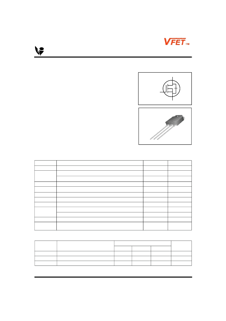
Symbol
2. Drain
3. Source
1. Gate
PROV IS IONAL
TO-247
G
S
D
相關PDF資料 |
PDF描述 |
|---|---|
| WG12232B | WG12232B |
| WG12232BG | WG12232B |
| WG12232E | PROFESSIONAL LCD MODULE MANUFACTURE |
| WG128128A | LCD MODULE GRAPHIC 128 X 128 DOTS |
| WG12864A | WINSTAR Professional LCD Module Manufacture |
相關代理商/技術參數 |
參數描述 |
|---|---|
| WFW9N90W | 制造商:WINSEMI 制造商全稱:WINSEMI 功能描述:Silicon N-Channel MOSFET |
| WFX2 | 制造商:RADIOMETRIX 制造商全稱:RADIOMETRIX 功能描述:500mW High power, fast, multi-channel transceiver |
| WFY03DN50 | 制造商:WINSEMI 制造商全稱:WINSEMI 功能描述:500V N?Channel Depletion-Mode DMOSFET |
| WFY3N02 | 制造商:WINSEMI 制造商全稱:WINSEMI 功能描述:20V N?Channel MOSFET |
| WFY3P02 | 制造商:WINSEMI 制造商全稱:WINSEMI 功能描述:−20V, P−Channel MOSFET |
發布緊急采購,3分鐘左右您將得到回復。