- 您現(xiàn)在的位置:買賣IC網(wǎng) > PDF目錄364009 > WS57C256F-35 (意法半導(dǎo)體) HIGH SPEED 32K x 8 CMOS EPROM PDF資料下載
參數(shù)資料
| 型號: | WS57C256F-35 |
| 廠商: | 意法半導(dǎo)體 |
| 英文描述: | HIGH SPEED 32K x 8 CMOS EPROM |
| 中文描述: | 高速32K的× 8的CMOS存儲器 |
| 文件頁數(shù): | 1/5頁 |
| 文件大小: | 49K |
| 代理商: | WS57C256F-35 |
WS57C256F
3-13
V
CC
A14
A13
A8
A9
A11
OE
A10
CE/PGM
O
7
O
6
O
5
O
4
O
3
V
PP
A
12
A
7
A
6
A
5
A
4
A
3
A
2
A
1
A
0
O
0
O
1
O
2
GND
1
2
3
4
5
6
7
8
9
10
11
12
13
14
28
27
26
25
24
23
22
21
20
19
18
17
16
15
A
8
A
9
A
11
NC
OE
A
10
CE/PGM
O
7
O
6
A
6
A
5
A
4
A
3
A
2
A
1
A
0
NC
O
0
A
7
A
1
V
P
N
V
C
A
1
A
1
O
1
O
2
NC
O
3
O
4
O
5
G
1
4 3
2
32 31 30
29
28
27
26
25
24
23
22
21
5
6
7
8
9
10
11
12
13
14 15 16 17 18 19 20
TOP VIEW
Chip Carrier
CERDIP
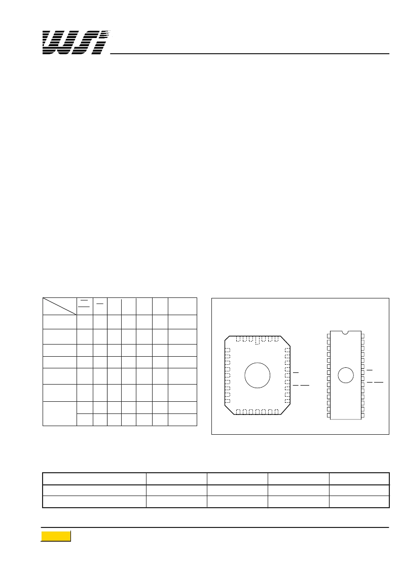
PIN CONFIGURATION
HIGH SPEED 32K x 8 CMOS EPROM
KEY FEATURES
Fast Access Time
— t
ACC
= 35 ns
— t
CE
= 35 ns
Low Power Consumption
— 200 μA Standby I
CC
Immune to Latch-UP
— Up to 200 mA
ESD Protection Exceeds 2000 Volts
Available in 300 Mil DIP and PLDCC
DESC SMD No. 5962-86063
GENERAL DESCRIPTION
The WS57C256F is a High Performance 32K x 8 UV Erasable EPROM. It is manufactured using an advanced
CMOS process technology enabling it to operate at speeds as fast as 35 ns Address Access Time (t
ACC
) and 35 ns
Chip Enable Time (t
CE
). It was designed utilizing WSI's patented self-aligned split gate EPROM cell, resulting in a
low power device with a very cost effective die size. The low standby power capability of this 256 K product (200 μA
in a CMOS interface environment) is especially attractive.
This product, with its high speed capability, is particularly appropriate for use with today's fast DSP processors and
high-clock-rate Microprocessors. The WS57C256F's 35 ns speed enables these advanced processors to operate
without introducing any undesirable wait states. The WS57C256F is also ideal for use in modem applications, and is
recommended for use in these applications by the leading modem chip set manufacturer.
The WS57C256F is available in a variety of package types including the space saving 300 Mil DIP, the surface
mount PLDCC, and other windowed and non-windowed options. And its standard JEDEC EPROM pinouts provide
for automatic upgrade density paths for current 64K and 128K EPROM users.
PINS
CE/
PGM
OE
A9
A0
VPP
VCCOUTPUTS
MODE
Read
VIL
VIL
X
X
VCCVCC
DOUT
Output
Disable
X
VIH
X
X
VCCVCC
High Z
Standby
VIH
X
X
X
VCCVCC
VPP
2
VCC
High Z
Program
VIL
VIH
X
X
DIN
Program
Verify
X
VIL
X
X
VPP
2
VCC
DOUT
Program
Inhibit
VIH
VIH
X
X
VPP
2
VCC
High Z
Signature
3
VIL
VIL
VH
2
VH
2
VIH
VIL
VCCVCC
23 H
4
VIL
VIL
VCCVCC
EO H
5
MODE SELECTION
NOTES:
1. X can be V
IL
or V
IH
.
2. V
IH
= V
PP
= 12.75 ± 0.25 V.
3. A1 – A8, A10 – A14 = V
IL
.
4. Manufacturer Signature.
5. Device Signature.
PRODUCT SELECTION GUIDE
PARAMETER
Address Access Time (Max)
Output Enable Time (Max)
WS57C256F-35
35 ns
15 ns
WS57C256F-45
45 ns
20 ns
WS57C256F-55
55 ns
25 ns
WS57C256F-70
70 ns
30 ns
Return to Main Menu
相關(guān)PDF資料 |
PDF描述 |
|---|---|
| WS57C256F-35C | HIGH SPEED 32K x 8 CMOS EPROM |
| WS57C256F-35D | HIGH SPEED 32K x 8 CMOS EPROM |
| WS57C256F-35J | HIGH SPEED 32K x 8 CMOS EPROM |
| WS57C256F-35L | HIGH SPEED 32K x 8 CMOS EPROM |
| WS57C256F-35P | HIGH SPEED 32K x 8 CMOS EPROM |
相關(guān)代理商/技術(shù)參數(shù) |
參數(shù)描述 |
|---|---|
| WS57C256F-35C | 制造商:STMICROELECTRONICS 制造商全稱:STMicroelectronics 功能描述:HIGH SPEED 32K x 8 CMOS EPROM |
| WS57C256F-35D | 制造商:STMICROELECTRONICS 制造商全稱:STMicroelectronics 功能描述:HIGH SPEED 32K x 8 CMOS EPROM |
| WS57C256F-35J | 制造商:STMICROELECTRONICS 制造商全稱:STMicroelectronics 功能描述:HIGH SPEED 32K x 8 CMOS EPROM |
| WS57C256F-35L | 制造商:STMICROELECTRONICS 制造商全稱:STMicroelectronics 功能描述:HIGH SPEED 32K x 8 CMOS EPROM |
| WS57C256F-35P | 制造商:STMICROELECTRONICS 制造商全稱:STMicroelectronics 功能描述:HIGH SPEED 32K x 8 CMOS EPROM |
發(fā)布緊急采購,3分鐘左右您將得到回復(fù)。