- 您現(xiàn)在的位置:買賣IC網(wǎng) > PDF目錄374964 > XC1704LVQ44C (XILINX INC) Configuration PROMs PDF資料下載
參數(shù)資料
| 型號(hào): | XC1704LVQ44C |
| 廠商: | XILINX INC |
| 元件分類: | DRAM |
| 英文描述: | Configuration PROMs |
| 中文描述: | 4M X 1 CONFIGURATION MEMORY, PQFP44 |
| 封裝: | PLASTIC, VQFP-44 |
| 文件頁數(shù): | 1/12頁 |
| 文件大小: | 124K |
| 代理商: | XC1704LVQ44C |
DS027 (v3.1) July 5, 2000
Product Specification
1-800-255-77781
2000 Xilinx, Inc. All rights reserved. All Xilinx trademarks, registered trademarks, patents, and disclaimers are as listed at
http://www.xilinx.com/legal.htm
.
All other trademarks and registered trademarks are the property of their respective owners. All specifications are subject to change without notice.
Features
One-time programmable (OTP) read-only memory
designed to store configuration bitstreams of Xilinx
FPGA devices
Simple interface to the FPGA; requires only one user
I/O pin
Cascadable for storing longer or multiple bitstreams
Programmable reset polarity (active High or active
Low) for compatibility with different FPGA solutions
XC17128E/EL, XC17256E/EL, XC1701 and XC1700L
series support fast configuration
Low-power CMOS Floating Gate process
XC1700E series are available in 5V and 3.3V versions
XC1700L series are available in 3.3V only
Available in compact plastic packages: 8-pin SOIC,
8-pin VOIC, 8-pin PDIP, 20-pin SOIC, 20-pin PLCC,
44-pin PLCC or 44-pin VQFP.
Programming support by leading programmer
manufacturers.
Design support using the Xilinx Alliance and
Foundation series software packages.
Guaranteed 20 year life data retention
Description
The XC1700 family of configuration PROMs provides an
easy-to-use, cost-effective method for storing large Xilinx
FPGA configuration bitstreams.
When the FPGA is in Master Serial mode, it generates a
configuration clock that drives the PROM. A short access
time after the rising clock edge, data appears on the PROM
DATA output pin that is connected to the FPGA D
IN
pin. The
FPGA generates the appropriate number of clock pulses to
complete the configuration. Once configured, it disables the
PROM. When the FPGA is in Slave Serial mode, the PROM
and the FPGA must both be clocked by an incoming signal.
Multiple devices can be concatenated by using the CEO
output to drive the CE input of the following device. The
clock inputs and the DATA outputs of all PROMs in this
chain are interconnected. All devices are compatible and
can be cascaded with other members of the family.
For device programming, either the Xilinx Alliance or Foun-
dation series development system compiles the FPGA
design file into a standard Hex format, which is then trans-
ferred to most commercial PROM programmers.
0
XC1700E and XC1700L Series
Configuration PROMs
DS027 (v3.1) July 5, 2000
0
8
Product Specification
R
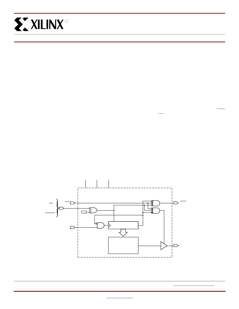
Figure 1:
Simplified Block Diagram (does not show programming circuit)
EPROM
Cell
Matrix
Address Counter
CE
DATA
OE
Output
CLK
VCC
VPP
GND
DS027_01_021500
TC
OE
or
RESET/
OE/
RESET
CEO
相關(guān)PDF資料 |
PDF描述 |
|---|---|
| XC1704LVQ44I | Configuration PROMs |
| XC17128ELPC20C | Configuration PROMs |
| XC17128ELPC20I | Configuration PROMs |
| XC17128ELPD8C | Configuration PROMs |
| XC17128ELPD8I | Configuration PROMs |
相關(guān)代理商/技術(shù)參數(shù) |
參數(shù)描述 |
|---|---|
| XC1704LVQ44I | 制造商:XILINX 制造商全稱:XILINX 功能描述:Configuration PROMs |
| XC17128DDD8M | 制造商:Xilinx 功能描述: |
| XC17128D-PC20C | 制造商:未知廠家 制造商全稱:未知廠家 功能描述:Configuration EPROM |
| XC17128D-PC20I | 制造商:未知廠家 制造商全稱:未知廠家 功能描述:Configuration EPROM |
| XC17128DPD8 | 制造商:Xilinx 功能描述: |
發(fā)布緊急采購,3分鐘左右您將得到回復(fù)。