- 您現(xiàn)在的位置:買賣IC網(wǎng) > PDF目錄376451 > XJ108-110 (CALOGIC LLC) N-Channel JFET Switch PDF資料下載
參數(shù)資料
| 型號: | XJ108-110 |
| 廠商: | CALOGIC LLC |
| 英文描述: | N-Channel JFET Switch |
| 中文描述: | N溝道場效應(yīng)開關(guān) |
| 文件頁數(shù): | 1/1頁 |
| 文件大小: | 21K |
| 代理商: | XJ108-110 |
N-Channel JFET Swtch
J108 – J110 /SST108 – SST110
FEATURES
Low Cost
Automated Insertion Package
Low Insertion Loss
No Offset or Error Voltages Generated by Closed Switch
Purely Resistive
High Isolation Resistance from Driver
Fast Switching
Low Noise
APPLICATIONS
Analog Switches
Choppers
Commutators
Low-Noise Audio Amplifiers
ABSOLUTE MAXIMUM RATINGS
(T
A
= 25
o
C unless otherwise specified)
Gate-Drain or Gate-Source Voltage . . . . . . . . . . . . . . . . -25V
Gate Current . . . . . . . . . . . . . . . . . . . . . . . . . . . . . . . . . 50mA
Storage Temperature Range . . . . . . . . . . . . . -55
o
C to +150
o
C
Operating Temperature Range . . . . . . . . . . . -55
o
C to +135
o
C
Lead Temperature (Soldering, 10sec). . . . . . . . . . . . . +300
o
C
Power Dissipation . . . . . . . . . . . . . . . . . . . . . . . . . . . . 360mW
Derate above 25
o
C . . . . . . . . . . . . . . . . . . . . . . . 3.3mW/
o
C
NOTE:
Stresses above those listed under "Absolute Maximum
Ratings" may cause permanent damage to the device. These are
stress ratings only and functional operation of the device at these or
any other conditions above those indicated in the operational sections
of the specifications is not implied. Exposure to absolute maximum
rating conditions for extended periods may affect device reliability.
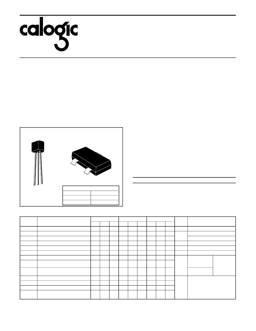
ORDERING INFORMATION
Part
J108-110
XJ108-110
SST109-110 Plastic SOT-23
Package
Plastic TO-92
Sorted Chips in Carriers
Temperature Range
-55
o
C to +135
o
C
-55
o
C to +135
o
C
-55
o
C to +135
o
C
C ORPORATION
PIN CONFIGURATION
TO-92
SG
D
5018
ELECTRICAL CHARACTERISTICS
(T
A
= 25
o
C unless otherwise specified)
SYMBOL
PARAMETER
108
TYP MAX MIN
-3
-10
109
TYP MAX MIN
-3
-6
110
TYP MAX
UNITS
TEST CONDITIONS
MIN
I
GSS
V
GS(off)
BV
GSS
I
DSS
I
D(off)
r
DS(on)
C
dg(off)
Gate Reverse Current (Note 1)
Gate-Source Cutoff Voltage
Gate-Source Breakdown Voltage
Drain Saturation Current (Note 2)
Drain Cutoff Current (Note 1)
Drain-Source ON Resistance
Drain-Gate OFF Capacitance
-3
-4
nA
V
DS
= 0V, V
GS
= -15V
V
DS
= 5V, I
D
= 1
μ
A
V
DS
= 0V, I
G
= -1
μ
A
V
DS
= 15V, V
GS
= 0V
V
DS
= 5V, V
GS
= -10V
V
DS
≤
0.1V, V
GS
= 0V
V
DS
= 0,
V
GS
= -10V
(Note 3)
V
DS
= V
GS
= 0
(Note 3)
Switching Time Test
Conditions (Note 3)
J107
V
DD
1.5V
V
GS(off)
-12V
R
L
150
-3
-25
80
-2
-25
40
-0.5
-25
10
V
mA
nA
3
8
15
3
12
15
3
18
15
pF
f = 1MHz
C
sg(off)
Source-Gate OFF Capacitance
15
15
15
C
dg(on)
+ C
sg(on)
t
d(on)
t
r
t
d(off)
Drain-Gate Plus Source-Gate
ON Capacitance
Turn On Delay Time
Rise Time
Turn OFF Delay Time
85
85
85
4
1
6
4
1
6
4
1
6
ns
J109
1.5V
-7V
150
J110
1.5V
-5V
150
t
f
Fall Time
30
30
30
NOTES: 1.
Approximately doubles for every 10
o
C increase in T
A
.
2.
Pulse test duration = 300
μ
s; duty cycle
≤
3%.
3.
For design reference only, not 100% tested.
PRODUCT MARKING (SOT-23)
SST108
SST109
SST110
I
08
I
09
I
10
SOT-23
G
S
D
相關(guān)PDF資料 |
PDF描述 |
|---|---|
| XM116 | Diode Protected N-Channel Enhancement Mode MOSFET General Purpose Amplifier |
| XPAD1-100 | Low Leakage Pico Amp Diodes |
| XPAD5-200 | Low Leakage Pico Amp Diodes |
| XR-1015 | Seventh Order Elliptic Low Pass Filters |
| XR-1016CD | Seventh Order Elliptic Low Pass Filters |
相關(guān)代理商/技術(shù)參數(shù) |
參數(shù)描述 |
|---|---|
| X-J1A-300L | 制造商:Leach International Corporation 功能描述:MID RANGE - Bulk |
| XJ1B107 | 制造商:LEACH 功能描述:New |
| X-J1B-107 | 制造商:Leach International Corporation 功能描述:84003-014 - Bulk |
| X-J1B-300L | 制造商:Leach International Corporation 功能描述:MID RANGE - Bulk |
| X-J1B-300M | 制造商:Leach International Corporation 功能描述:MID RANGE - Bulk |
發(fā)布緊急采購,3分鐘左右您將得到回復。