- 您現在的位置:買賣IC網 > PDF目錄376459 > XRK4993IR-2 (EXAR CORP) 3.3V PROGRAMMABLE SKEW CLOCK BUFFER PDF資料下載
參數資料
| 型號: | XRK4993IR-2 |
| 廠商: | EXAR CORP |
| 元件分類: | 時鐘及定時 |
| 英文描述: | 3.3V PROGRAMMABLE SKEW CLOCK BUFFER |
| 中文描述: | 4993 SERIES, PLL BASED CLOCK DRIVER, 8 TRUE OUTPUT(S), 0 INVERTED OUTPUT(S), PDSO28 |
| 封裝: | 0.150 INCH, QSOP-28 |
| 文件頁數: | 1/13頁 |
| 文件大小: | 95K |
| 代理商: | XRK4993IR-2 |
Exar
Corporation 48720 Kato Road, Fremont CA, 94538
(510) 668-7000
FAX (510) 668-7017
www.exar.com
XRK4993
3.3V PROGRAMMABLE SKEW CLOCK BUFFER
FEBRUARY 2007
REV. 1.0.0
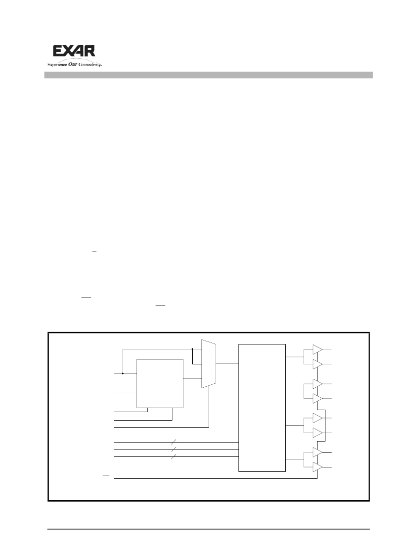
FUNCTIONAL DESCRIPTION
The XRK4993 is a 3.3V High-Speed Low-Voltage
Programmable Skew Clock Buffer. It is intended for
high-performance computer systems and offers user
selectable control over system clock functions to
optimize timing. Eight ouputs, arranged in four
banks, can each drive 75
Ω
terminated transmission
lines while delivering minimal and specified output
skews and full-swing Low Voltage TTL logic levels.
Banks A, B, C (two outputs per bank) can be
individually selected for one of nine delay or function
configurations through two dedicated three-level
inputs. These outputs are able to lead or lag the
CLKIN input reference clock by up to 6 time units
from their nominal "zero" skew position. The
integrated PLL allows external load and transmission
line delay effects to be canceled achieving zero delay
capability. Combining the zero delay capability with
the selectable output skew functions, output-to-output
delays of up to +12 time units can be created.
The XRK4993’s divide functions (divide-by-two and
divide-by-four) allow distribution of a low-frequency
clock that can be multiplied by two or four at the clock
destination. This feature facilitates clock distribution
while allowing maximum system clock flexibility.
When the OE pin is held low, all the outputs are
synchronously enabled. However, if OE is held high,
all the outputs except QC0 and QC1 are
synchronously disabled.
When PE is held high, all the outputs are
synchronized with the positive edge of the CLKIN
clock input. When PE is held low, all the outputs are
synchronized with the negative edge of CLKIN. The
device has LVTTL outputs with 12mA balanced drive.
FEATURES
3 pairs of programmable skew outputs
Low skew: 200ps same pair, 250ps all outputs
Selectable
positive
synchronization: Excellent for DSP applications
Synchronous output enable
Output frequency: 3.75MHz to 85MHz
2x, 4x, 1/2, and 1/4 output frequencies
3 skew grades
3-level inputs for skew and PLL range control
PLL bypass mode
External feedback, internal loop filter
12mA balanced drive outputs
Available in 28 pin QSOP package
Jitter < 200 ps peak-to-peak
CLKIN input is 5V tolerant
or
negative
edge
F
IGURE
1. B
LOCK
D
IAGRAM
OF
THE
XRK4993
SELC
PLL
CLKIN
FSEL*
PLL_BYPASS*
Bank “SKEW”
Control
QA0
QA1
QB0
QB1
QC0
QC1
QD0
QD1
SELA[1:0]*
SELB[1:0]*
[1:0]*
L
M
H
Ref
Feedback
2
2
2
FB_IN
PE
OE
* Three-level inputs
相關PDF資料 |
PDF描述 |
|---|---|
| XRK4993IR-5 | 3.3V PROGRAMMABLE SKEW CLOCK BUFFER |
| XRK69772 | 1:12 LVCMOS PLL CLOCK GENERATOR |
| XRK69772CR | 1:12 LVCMOS PLL CLOCK GENERATOR |
| XRK69772IR | 1:12 LVCMOS PLL CLOCK GENERATOR |
| XRK69773 | 1:12 LVCMOS PLL CLOCK GENERATOR |
相關代理商/技術參數 |
參數描述 |
|---|---|
| XRK4993IR-5 | 制造商:EXAR 制造商全稱:EXAR 功能描述:3.3V PROGRAMMABLE SKEW CLOCK BUFFER |
| XRK4993IR-7 | 制造商:EXAR 制造商全稱:EXAR 功能描述:3.3V PROGRAMMABLE SKEW CLOCK BUFFER |
| XRK69772 | 制造商:EXAR 制造商全稱:EXAR 功能描述:1:12 LVCMOS PLL CLOCK GENERATOR |
| XRK69772CR | 制造商:EXAR 制造商全稱:EXAR 功能描述:1:12 LVCMOS PLL CLOCK GENERATOR |
| XRK69772IR | 制造商:EXAR 制造商全稱:EXAR 功能描述:1:12 LVCMOS PLL CLOCK GENERATOR |
發布緊急采購,3分鐘左右您將得到回復。