- 您現在的位置:買賣IC網 > PDF目錄208010 > 5962H0521404VXA 200 MHz, OTHER CLOCK GENERATOR, CDFP48 PDF資料下載
參數資料
| 型號: | 5962H0521404VXA |
| 元件分類: | XO, clock |
| 英文描述: | 200 MHz, OTHER CLOCK GENERATOR, CDFP48 |
| 封裝: | CERAMIC, DFP-48 |
| 文件頁數: | 1/22頁 |
| 文件大小: | 174K |
| 代理商: | 5962H0521404VXA |
1
FEATURES:
+3.3V Core Power Supply
+2.5V or +3.3V Clock Output Power Supply
- Independent Clock Output Bank Power Supplies
Output frequency range: 6 MHz to 200 MHz
Bank pair output-output skew < 100 ps
Cycle-cycle jitter < 50 ps
50% ± 2% maximum output duty cycle at 100MHz
Eight LVTTL outputs with selectable drive strength
Selectable positive- or negative-edge synchronization
Selectable phase-locked loop (PLL) frequency range and
lock indicator
Phase adjustments in 625 to 1300 ps steps up to ± 7.8 ns
(1-6,8,10,12) x multiply and (1/2,1/4) x divide ratios
Compatible with Spread-Spectrum reference clocks
Power-down mode
Selectable reference input divider
Operational environment:
- Total-dose tolerance: 100 krad (Si)
- SEL Immune to a LET of 109 MeV-cm2/mg
- SEU Immune to a LET of 109 MeV-cm2/mg
HiRel temperature range: -55oC to +125oC
Extended industrial temp: -40oC to +125oC
Packaging options:
- 48-Lead Ceramic Flatpack
- 48-Lead QFNdevelopment pending/contact factory
Standard Microcircuit Drawing: 5962-05214
- QML-Q and QML-V compliant part
INTRODUCTION:
The UT7R995/UT7R995C is a low-voltage, low-power, eight-
output, 6-to-200 MHz clock driver. It features output phase
programmability which is necessary to optimize the timing of
high-performance microprocessor and communication sys-
tems.
The user programs both the frequency and the phase of the out-
put banks through nF[1:0] and DS[1:0] pins. The adjustable
phase feature allows the user to skew the outputs to lead or lag
the reference clock. Connect any one of the outputs to the
feedback input to achieve different reference frequency multi-
plication and division ratios.
The devices also feature split output bank power supplies that
enable banks 1 & 2, bank 3, and bank 4 to operate at a different
power supply levels. The ternary PE/HD pin controls the syn-
chronization of output signals to either the rising or the falling
edge of the reference clock and selects the drive strength of the
output buffers.
To ensure smooth startup of the UT7R995/UT7R995C, inde-
pendent of the behavior of the reference clock, it is recom-
mended that the PD/DIV pin be held low to reset the device
until power up is complete and the reference clock is stable.
Similarly, if the frequency range select pin (FS) is changed
during operation of the UT7R995/UT7R995C, the PD/DIV
must be driven low for a minimum of 3
μs to guarantee the
transition from one FS range to the next, ensuring the reliable
start up of the newly selected PLL oscillator.
The UT7R995 and UT7R995C both interface to a digital clock
while the UT7R995C will also interface to a quartz crystal.
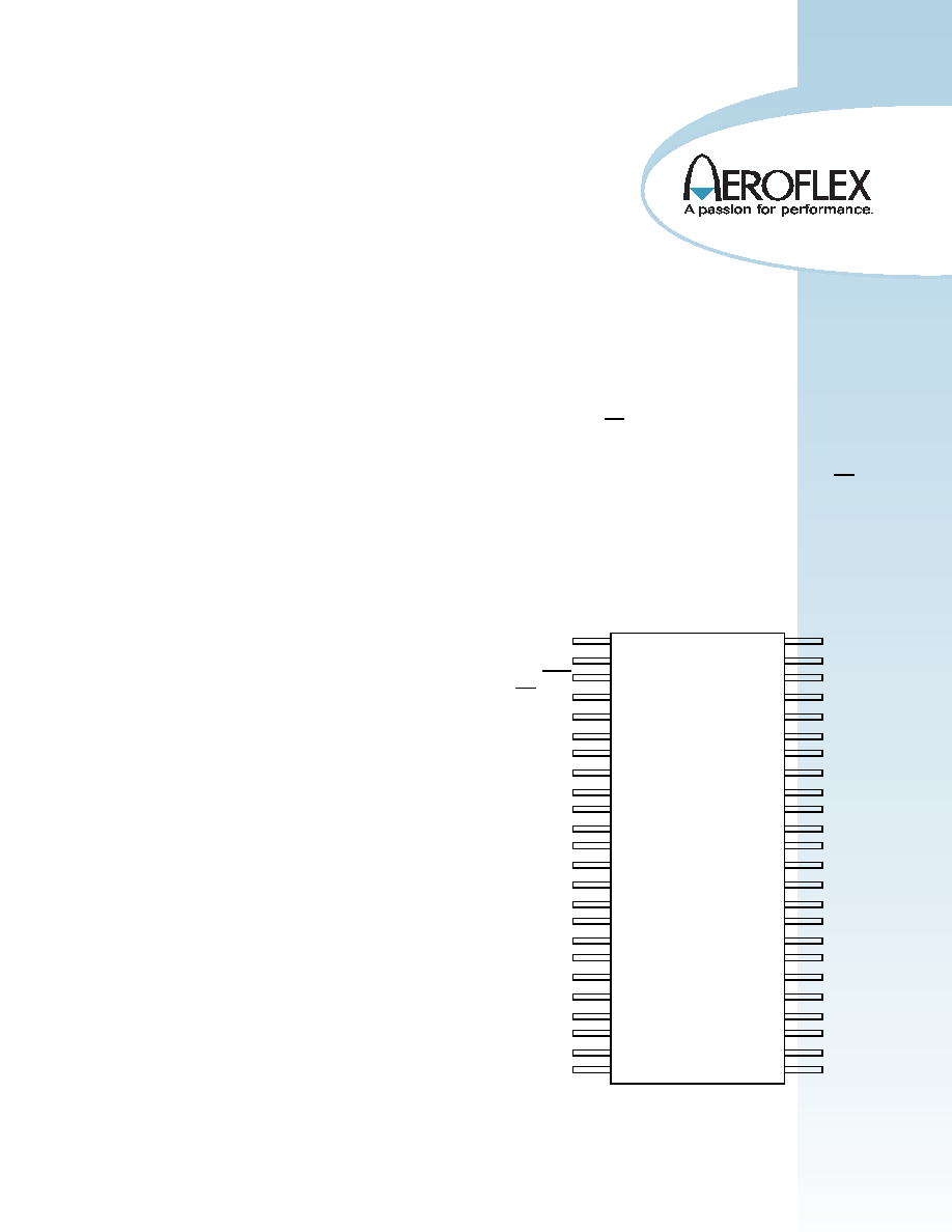
Figure 1. 48-Lead Ceramic Flatpack Pin Description
1
2
3
4
5
6
7
8
9
10
11
12
13
14
15
16
17
18
19
20
21
22
23
24
48
47
46
45
44
43
42
41
40
39
38
37
36
35
34
33
32
31
30
29
28
27
26
25
4F0
4F1
sOE
PD/DIV
PE/HD
VDD
VDDQ3
3Q1
3Q0
VSS
VDD
FB
VDD
VSS
2Q1
2Q0
VDDQ1
LOCK
VSS
DS0
DS1
1F0
3F1
3F0
FS
VSS
VDDQ4
4Q1
4Q0
VSS
VDD
XTAL1
NC/XTAL2
VDD
VSS
1Q1
1Q0
VDDQ1
VSS
TEST
2F1
2F0
1F1
UT7R995
&
UT7R995C
Standard Products
UT7R995 & UT7R995C RadClockTM
2.5V/3.3V 200MHz High-Speed
Multi-phase PLL Clock Buffer
Datasheet
August 2009
相關PDF資料 |
PDF描述 |
|---|---|
| 514DCAXXXXXXBAG | 250 MHz, OTHER CLOCK GENERATOR, PDSO6 |
| 514ECCXXXXXXAAGR | 125 MHz, OTHER CLOCK GENERATOR, PDSO6 |
| 514KCAXXXXXXBAGR | 250 MHz, OTHER CLOCK GENERATOR, PDSO6 |
| 514QBCXXXXXXBAGR | 125 MHz, OTHER CLOCK GENERATOR, PDSO6 |
| 514SCCXXXXXXAAG | 125 MHz, OTHER CLOCK GENERATOR, PDSO6 |
相關代理商/技術參數 |
參數描述 |
|---|---|
| 5962H94A0305QXC | 制造商: 功能描述: 制造商:undefined 功能描述: |
| 5962H9853701 | 制造商: 功能描述: 制造商:undefined 功能描述: |
| 5962L0051502VHA | 制造商:Analog Devices 功能描述:AEROSPACE 7NS SINGLE COMPARATOR - Trays |
| 5962L0052401VGA | 功能描述:校驗器 IC RoHS:否 制造商:STMicroelectronics 產品: 比較器類型: 通道數量: 輸出類型:Push-Pull 電源電壓-最大:5.5 V 電源電壓-最小:1.1 V 補償電壓(最大值):6 mV 電源電流(最大值):1350 nA 響應時間: 最大工作溫度:+ 125 C 安裝風格:SMD/SMT 封裝 / 箱體:SC-70-5 封裝:Reel |
| 5962L0052401VHA | 功能描述:校驗器 IC RoHS:否 制造商:STMicroelectronics 產品: 比較器類型: 通道數量: 輸出類型:Push-Pull 電源電壓-最大:5.5 V 電源電壓-最小:1.1 V 補償電壓(最大值):6 mV 電源電流(最大值):1350 nA 響應時間: 最大工作溫度:+ 125 C 安裝風格:SMD/SMT 封裝 / 箱體:SC-70-5 封裝:Reel |
發布緊急采購,3分鐘左右您將得到回復。