- 您現在的位置:買賣IC網 > PDF目錄68800 > 5962R9673801QDA (NATIONAL SEMICONDUCTOR CORP) QUAD COMPARATOR, 4000 uV OFFSET-MAX, 1300 ns RESPONSE TIME, CDFP14 PDF資料下載
參數資料
| 型號: | 5962R9673801QDA |
| 廠商: | NATIONAL SEMICONDUCTOR CORP |
| 元件分類: | 比較器 |
| 英文描述: | QUAD COMPARATOR, 4000 uV OFFSET-MAX, 1300 ns RESPONSE TIME, CDFP14 |
| 封裝: | W14B |
| 文件頁數: | 16/20頁 |
| 文件大小: | 380K |
| 代理商: | 5962R9673801QDA |
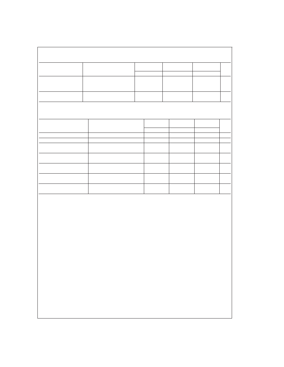
Electrical Characteristics (Continued)
(V
+ = 5.0 V
DC, (Note 7))
Parameter
Conditions
LM139A
LM239A,
LM339A
LM139
Units
Min Typ
Max
Min
Typ
Max
Min Typ
Max
Output Leakage Current
V
IN(+)=1VDC,VIN()=0,
1.0
A
DC
V
O=30 VDC, (LM3302,
V
O=28 VDC)
Differential Input Voltage
Keep all V
IN’s≥0VDC (or V
,36
36
V
DC
if used), (Note 11)
Electrical Characteristics
(V
+ = 5.0 V
DC, (Note 7))
Parameter
Conditions
LM239,
LM339
LM2901
LM3302
Units
Min Typ
Max
Min Typ
Max
Min Typ
Max
Input Offset Voltage
(Note 12)
9.0
9
15
40
mV
DC
Input Offset Current
I
IN(+)IIN(),VCM=0V
150
50
200
300
nA
DC
Input Bias Current
I
IN(+) or IIN() with Output in
400
200
500
1000
nA
DC
Linear Range, V
CM=0V (Note 8)
Input Common-Mode
V
+=30 V
DC (LM3302, V
+=28 V
DC)V
+2.0
0
V
+2.0
0
V
+2.0
V
DC
Voltage Range
(Note 9)
Saturation Voltage
V
IN()=1VDC,VIN(+)=0,
700
400
700
mV
DC
I
SINK≤4mA
Output Leakage Current
V
IN(+)=1VDC,VIN()=0,
1.0
A
DC
V
O=30 VDC, (LM3302, VO=28 VDC)
Differential Input Voltage
Keep all V
IN’s≥0VDC (or V
,
363628
V
DC
if used), (Note 11)
Note 4: For operating at high temperatures, the LM339/LM339A, LM2901, LM3302 must be derated based on a 125C maximum junction temperature and a thermal
resistance of 95C/W which applies for the device soldered in a printed circuit board, operating in a still air ambient. The LM239 and LM139 must be derated based
on a 150C maximum junction temperature. The low bias dissipation and the “ON-OFF” characteristic of the outputs keeps the chip dissipation very small(PD≤100
mW), provided the output transistors are allowed to saturate.
Note 5: Short circuits from the output to V+ can cause excessive heating and eventual destruction. When considering short circuits to ground, the maximum output
current is approximately 20 mA independent of the magnitude of V+.
Note 6: This input current will only exist when the voltage at any of the input leads is driven negative. It is due to the collector-base junction of the input PNP tran-
sistors becoming forward biased and thereby acting as input diode clamps. In addition to this diode action, there is also lateral NPN parasitic transistor action on the
IC chip. This transistor action can cause the output voltages of the comparators to go to the V+ voltage level (or to ground for a large overdrive) for the time duration
that an input is driven negative. This is not destructive and normal output states will re-establish when the input voltage, which was negative, again returns to a value
greater than 0.3 VDC (at 25)C.
Note 7: These specifications are limited to 55C
≤TA≤+125C, for the LM139/LM139A. With the LM239/LM239A, all temperature specifications are limited to
25C
≤TA≤+85C, the LM339/LM339A temperature specifications are limited to 0C≤TA≤+70C, and the LM2901, LM3302 temperature range is 40C≤TA≤+85C.
Note 8: The direction of the input current is out of the IC due to the PNP input stage. This current is essentially constant, independent of the state of the outputso
no loading change exists on the reference or input lines.
Note 9: The input common-mode voltage or either input signal voltage should not be allowed to go negative by more than 0.3V. The upper end of the common-mode
voltage range is V+ 1.5V at 25C, but either or both inputs can go to +30 VDC without damage (25V for LM3302), independent of the magnitude of V
+.
Note 10: The response time specified is a 100 mV input step with 5 mV overdrive. For larger overdrive signals 300 ns can be obtained, see typical performance char-
acteristics section.
Note 11: Positive excursions of input voltage may exceed the power supply level. As long as the other voltage remains within the common-mode range, the com-
parator will provide a proper output state. The low input voltage state must not be less than 0.3 VDC (or 0.3 VDCbelow the magnitude of the negative power supply,
if used) (at 25C).
Note 12: At output switch point, VO1.4 VDC,RS=0 with V
+ from 5 V
DC to 30 VDC; and over the full input common-mode range (0 VDC to V
+ 1.5 V
DC), at 25C.
For LM3302, V+ from 5 VDC to 28 VDC.
Note 13: Refer to RETS139AX for LM139A military specifications and to RETS139X for LM139 military specifications.
www.national.com
5
相關PDF資料 |
PDF描述 |
|---|---|
| 5962R9673801QCA | QUAD COMPARATOR, 4000 uV OFFSET-MAX, 1300 ns RESPONSE TIME, CDIP14 |
| 5962R9673801QXA | QUAD COMPARATOR, 4000 uV OFFSET-MAX, 1300 ns RESPONSE TIME, CDSO14 |
| 5962R9679801QCA | DUAL COMPARATOR, 6800 uV OFFSET-MAX, 80 ns RESPONSE TIME, CDIP14 |
| 5962R9679801QHA | DUAL COMPARATOR, 6800 uV OFFSET-MAX, 80 ns RESPONSE TIME, CDSO10 |
| 5962R9679801QIA | DUAL COMPARATOR, 6800 uV OFFSET-MAX, 80 ns RESPONSE TIME, MBCY10 |
相關代理商/技術參數 |
參數描述 |
|---|---|
| 5962R9673801VCA | 功能描述:校驗器 IC RoHS:否 制造商:STMicroelectronics 產品: 比較器類型: 通道數量: 輸出類型:Push-Pull 電源電壓-最大:5.5 V 電源電壓-最小:1.1 V 補償電壓(最大值):6 mV 電源電流(最大值):1350 nA 響應時間: 最大工作溫度:+ 125 C 安裝風格:SMD/SMT 封裝 / 箱體:SC-70-5 封裝:Reel |
| 5962R9673801VDA | 功能描述:校驗器 IC RoHS:否 制造商:STMicroelectronics 產品: 比較器類型: 通道數量: 輸出類型:Push-Pull 電源電壓-最大:5.5 V 電源電壓-最小:1.1 V 補償電壓(最大值):6 mV 電源電流(最大值):1350 nA 響應時間: 最大工作溫度:+ 125 C 安裝風格:SMD/SMT 封裝 / 箱體:SC-70-5 封裝:Reel |
| 5962R9673801VXA | 制造商:Texas Instruments 功能描述:COMPARATOR QUAD 15V/30V 14PIN CPAK - Rail/Tube |
| 5962R9673802VCA | 功能描述:校驗器 IC RoHS:否 制造商:STMicroelectronics 產品: 比較器類型: 通道數量: 輸出類型:Push-Pull 電源電壓-最大:5.5 V 電源電壓-最小:1.1 V 補償電壓(最大值):6 mV 電源電流(最大值):1350 nA 響應時間: 最大工作溫度:+ 125 C 安裝風格:SMD/SMT 封裝 / 箱體:SC-70-5 封裝:Reel |
| 5962R9673802VDA | 功能描述:校驗器 IC RoHS:否 制造商:STMicroelectronics 產品: 比較器類型: 通道數量: 輸出類型:Push-Pull 電源電壓-最大:5.5 V 電源電壓-最小:1.1 V 補償電壓(最大值):6 mV 電源電流(最大值):1350 nA 響應時間: 最大工作溫度:+ 125 C 安裝風格:SMD/SMT 封裝 / 箱體:SC-70-5 封裝:Reel |
發布緊急采購,3分鐘左右您將得到回復。