- 您現在的位置:買賣IC網 > PDF目錄68811 > 71M6532F-IGTR/F (MAXIM INTEGRATED PRODUCTS INC) 1-CHANNEL POWER SUPPLY MANAGEMENT CKT, PQFP100 PDF資料下載
參數資料
| 型號: | 71M6532F-IGTR/F |
| 廠商: | MAXIM INTEGRATED PRODUCTS INC |
| 元件分類: | 電源管理 |
| 英文描述: | 1-CHANNEL POWER SUPPLY MANAGEMENT CKT, PQFP100 |
| 封裝: | LEAD FREE, LQFP-100 |
| 文件頁數: | 27/120頁 |
| 文件大小: | 2477K |
| 代理商: | 71M6532F-IGTR/F |
第1頁第2頁第3頁第4頁第5頁第6頁第7頁第8頁第9頁第10頁第11頁第12頁第13頁第14頁第15頁第16頁第17頁第18頁第19頁第20頁第21頁第22頁第23頁第24頁第25頁第26頁當前第27頁第28頁第29頁第30頁第31頁第32頁第33頁第34頁第35頁第36頁第37頁第38頁第39頁第40頁第41頁第42頁第43頁第44頁第45頁第46頁第47頁第48頁第49頁第50頁第51頁第52頁第53頁第54頁第55頁第56頁第57頁第58頁第59頁第60頁第61頁第62頁第63頁第64頁第65頁第66頁第67頁第68頁第69頁第70頁第71頁第72頁第73頁第74頁第75頁第76頁第77頁第78頁第79頁第80頁第81頁第82頁第83頁第84頁第85頁第86頁第87頁第88頁第89頁第90頁第91頁第92頁第93頁第94頁第95頁第96頁第97頁第98頁第99頁第100頁第101頁第102頁第103頁第104頁第105頁第106頁第107頁第108頁第109頁第110頁第111頁第112頁第113頁第114頁第115頁第116頁第117頁第118頁第119頁第120頁
Data Sheet 71M6531D/F-71M6532D/F
FDS 6531/6532 005
14
2005-2010 TERIDIAN Semiconductor Corporation
v1.3
the number of multiplexer frames in an accumulation interval is always even. Operation with
CHOP_E[1:0] = 00 does not require control of the chopping mechanism by the MPU while eliminating the
offset for temperature measurement.
In the second toggle state, CHOP_E[1:0] = 11, no ALT frame is forced during the last multiplexer cycle in
an accumulation interval and CROSS always toggles near the end of each multiplexer frame.
The internal bias voltage, VBIAS (typically 1.6 V), is used by the ADC when measuring the temperature
and battery monitor signals.
1.2.6
Temperature Sensor
The 71M6531D/F and 71M6532D/F include an on-chip temperature sensor implemented as a bandgap
reference. It is used to determine the die temperature. The MPU may request an alternate multiplexer
cycle containing the temperature sensor output by asserting MUX_ALT.
The primary use of the temperature data is to determine the magnitude of compensation required to offset
the thermal drift in the system (see Section 3.4 Temperature Compensation).
1.2.7
Battery Monitor
The battery voltage is measured by the ADC during alternative multiplexer frames if the BME (Battery
Measure Enable) bit in the I/O RAM is set. While BME is set, an on-chip 45 k
load resistor is applied to
the battery and a scaled fraction of the battery voltage is applied to the ADC input. After each alternative
MUX frame, the result of the ADC conversion is available at XRAM address 0x0B. BME is ignored and
assumed zero when system power is not available (V1 < VBIAS). See Section 5.4.4 Battery Monitor.
1.2.8
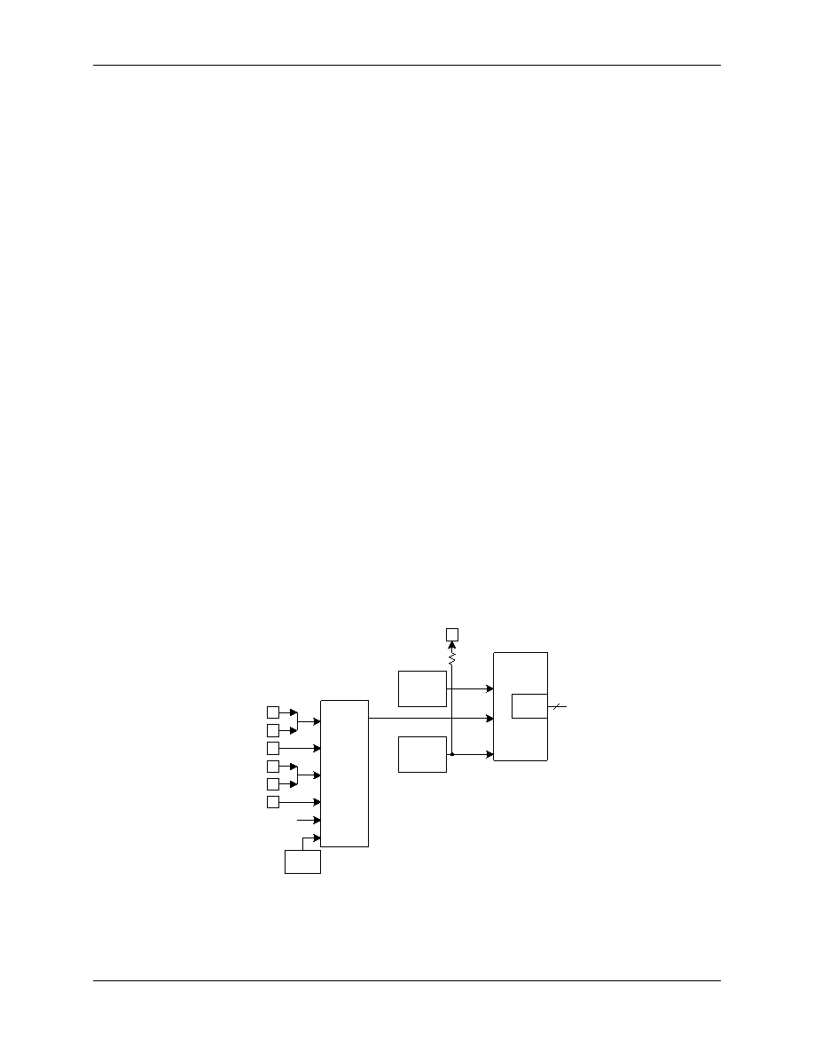
AFE Functional Description
The AFE functions as a data acquisition system, controlled by the MPU. The main signals (IA, VA, IB and
VB) are sampled, and the ADC counts obtained are stored in XRAM where they can be accessed by the
CE and, if necessary, by the MPU. Alternate multiplexer cycles are initiated less frequently by the MPU to
gather access to the slow temperature and battery signals.
Figure 5 shows the block diagram of the AFE, with current inputs shown only as differential pair of pins
(for the 71M6531D/F, the current input for phase A is a single pin [IA]).
Figure 5: AFE Block Diagram (Shown for the 71M6532D/F)
Σ ADC
CONVERTER
VREF
ADC_E
MUX
VREF
VBIAS
VREF
VREF_DIS
VBIAS
VREF_CAL
VBAT
VADC
MUX_DIV
MUX_ALT
EQU
22
FIR
FIR_LEN
VA
IBP
VB
IAP
IAN
IBN
TEMP
SENSOR
相關PDF資料 |
PDF描述 |
|---|---|
| 71M6534-IGT/F | SPECIALTY ANALOG CIRCUIT, PQFP120 |
| 71M6534H-IGTR/F | SPECIALTY ANALOG CIRCUIT, PQFP120 |
| 71M6533H-IGTR/F | SPECIALTY ANALOG CIRCUIT, PQFP100 |
| 71M6534-IGTR/F | SPECIALTY ANALOG CIRCUIT, PQFP120 |
| 71M6534H-IGT/F | SPECIALTY ANALOG CIRCUIT, PQFP120 |
相關代理商/技術參數 |
參數描述 |
|---|---|
| 71M6533 | 制造商:TERIDIAN 制造商全稱:TERIDIAN 功能描述:Energy Meter IC |
| 71M6533-DB | 功能描述:開發板和工具包 - 8051 71M6533 Demo Brd RoHS:否 制造商:Silicon Labs 產品:Development Kits 工具用于評估:C8051F960, Si7005 核心: 接口類型:USB 工作電源電壓: |
| 71M6533G | 制造商:MAXIM 制造商全稱:Maxim Integrated Products 功能描述:Exceeds IEC 62053/ANSI C12.20 Standards |
| 71M6533G-IGTR/F | 功能描述:計量片上系統 - SoC AC Power Monitoring SoC-Programd RoHS:否 制造商:Maxim Integrated 核心:80515 MPU 處理器系列:71M6511 類型:Metering SoC 最大時鐘頻率:70 Hz 程序存儲器大小:64 KB 數據 RAM 大小:7 KB 接口類型:UART 可編程輸入/輸出端數量:12 片上 ADC: 安裝風格:SMD/SMT 封裝 / 箱體:LQFP-64 封裝:Reel |
| 71M6533H | 制造商:TERIDIAN 制造商全稱:TERIDIAN 功能描述:Energy Meter IC |
發布緊急采購,3分鐘左右您將得到回復。