- 您現在的位置:買賣IC網 > PDF目錄68812 > 73M1903C-IM/F (MAXIM INTEGRATED PRODUCTS INC) SPECIALTY CONSUMER CIRCUIT, PQCC32 PDF資料下載
參數資料
| 型號: | 73M1903C-IM/F |
| 廠商: | MAXIM INTEGRATED PRODUCTS INC |
| 元件分類: | 消費家電 |
| 英文描述: | SPECIALTY CONSUMER CIRCUIT, PQCC32 |
| 封裝: | LEAD FREE, QFN-32 |
| 文件頁數: | 46/48頁 |
| 文件大小: | 487K |
| 代理商: | 73M1903C-IM/F |
第1頁第2頁第3頁第4頁第5頁第6頁第7頁第8頁第9頁第10頁第11頁第12頁第13頁第14頁第15頁第16頁第17頁第18頁第19頁第20頁第21頁第22頁第23頁第24頁第25頁第26頁第27頁第28頁第29頁第30頁第31頁第32頁第33頁第34頁第35頁第36頁第37頁第38頁第39頁第40頁第41頁第42頁第43頁第44頁第45頁當前第46頁第47頁第48頁
DS_1903C_033
73M1903C Data Sheet
Rev. 5.0
7
2.1
Serial Data and Control
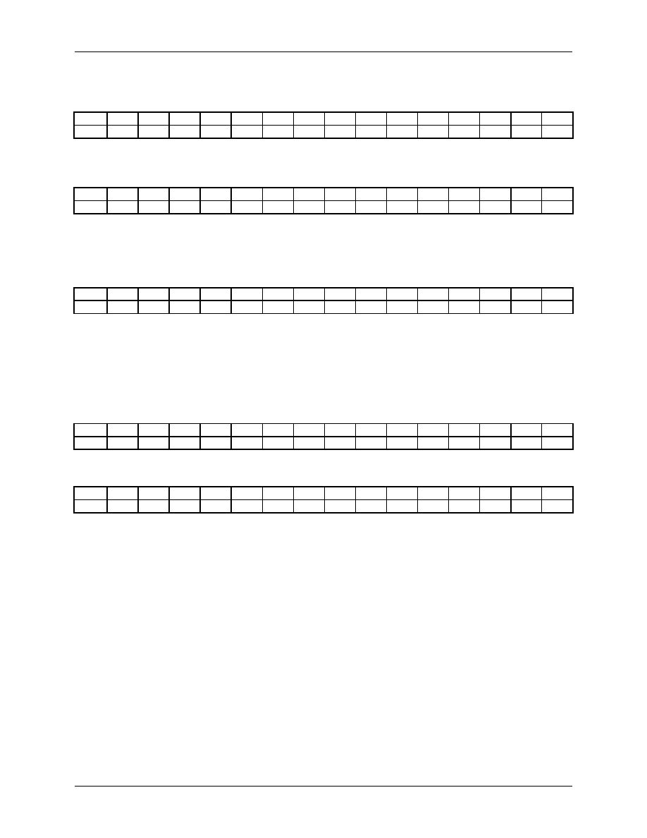
The bits transmitted on the SDOUT pin are defined as follows:
Bit15 Bit14 Bit13 Bit12 Bit11 Bit10
Bit9
Bit8
Bit7
Bit6
Bit5
Bit4
Bit3
Bit2
Bit1
Bit0
RX15 RX14 RX13 RX12 RX11 RX10 RX9
RX8
RX7
RX6
RX5
RX4
RX3
RX2
RX1
RX0
If the HC bit (Bit 0 of Register 01) is set to zero, the 16 bits that are received on the SDIN are defined as
follows:
Bit15 Bit14 Bit13 Bit12 Bit11 Bit10
Bit9
Bit8
Bit7
Bit6
Bit5
Bit4
Bit3
Bit2
Bit1
Bit0
TX15 TX14 TX13 TX12 TX11 TX10 TX9
TX8
TX7
TX6
TX5
TX4
TX3
TX2
TX1
CTL
In this case LSB(TX0) in a transmit bit stream is forced to 0 automatically.
If the Hardware Control bit (Bit 0 of Register 01) is set to one, the 16 bits that are received on the SDIN
input are defined as follows:
Bit15 Bit14 Bit13 Bit12 Bit11 Bit10
Bit9
Bit8
Bit7
Bit6
Bit5
Bit4
Bit3
Bit2
Bit1
Bit0
TX15 TX14 TX13 TX12 TX11 TX10 TX9
TX8
TX7
TX6
TX5
TX4
TX3
TX2
TX1
TX0
Bit 15 is transmitted/received first. Bits RX15:0 are the receive code word. Bits TX15:0 are the transmit
code word. If the hardware control bit is set to one, a control frame is initiated between every pair of data
frames. If the hardware control bit is set to zero, CTL is used by software to request a control frame. If
CTL is high, a control frame will be initiated before the next data frame. A control frame allows the
controller to read or write status and control to the 73M1903C.
The control word received on the SDIN pin is defined as follows:
Bit15 Bit14 Bit13 Bit12 Bit11 Bit10
Bit9
Bit8
Bit7
Bit6
Bit5
Bit4
Bit3
Bit2
Bit1
Bit0
R/W
A6
A5
A4
A3
A2
A1
A0
D7
D6
D5
D4
D3
D2
D1
D0
The control word transmitted on the SDOUT pin is defined as follows:
Bit15 Bit14 Bit13 Bit12 Bit11 Bit10
Bit9
Bit8
Bit7
Bit6
Bit5
Bit4
Bit3
Bit2
Bit1
Bit0
0
D7
D6
D5
D4
D3
D2
D1
D0
If the R/W bit (Bit15 of control word) is set to a 0, the data byte transmitted on the SDOUT pin is all zeros
and the data received on the SDIN pin is written to the register pointed to by the received address bits;
A6-A0. If the R/W bit is set to a 1, there is no write to any register and the data byte transmitted on the
SDOUT pin is the data contained in the register pointed to by address bits A6-A0. Only one control frame
can occur between any two data frames.
Writes to unimplemented registers are ignored. Reading an unimplemented register returns an unknown
value. The position of a control data frame is controlled by the SPOS; bit 1 of register 01h. If SPOS is
set to a 0 the control frames occur mid way between data frames, i.e., the time between data frames is
equal. If SPOS is set to a 1, the control frame is of the way between consecutive data frames, i.e., the
control frame is closer to the first data frame. This is illustrated in Figure 2.
The 73M1903C IC includes a feature that shuts off the serial clock (SCLK) after 32 cycles of SCLK
following the frame synch (Figure 1). The SckMode pin controls this mode. If this pin is left open, the
clock will run continuously. If SckMode is set low, the clock will be gated on for 32 clocks for each FS.
The SDOUT and
FS pins change values following a rising edge of SCLK. The SDIN pin is sampled on
the falling edge of SCLK. Figure 3 shows the timing diagrams for the serial port.
相關PDF資料 |
PDF描述 |
|---|---|
| 73M1903C-IMR/F | SPECIALTY CONSUMER CIRCUIT, PQCC32 |
| 73M1903C-IM | SPECIALTY CONSUMER CIRCUIT, QCC32 |
| 73M1903C-IM | SPECIALTY CONSUMER CIRCUIT, QCC32 |
| 73S1209F-44IM/F | POWER SUPPLY MANAGEMENT CKT, QCC44 |
| 73S1209F-68IM/F | POWER SUPPLY MANAGEMENT CKT, QCC68 |
相關代理商/技術參數 |
參數描述 |
|---|---|
| 73M1903C-IMR/F | 功能描述:電信線路管理 IC Modem Analog Front End RoHS:否 制造商:STMicroelectronics 產品:PHY 接口類型:UART 電源電壓-最大:18 V 電源電壓-最小:8 V 電源電流:30 mA 最大工作溫度:+ 85 C 最小工作溫度:- 40 C 安裝風格:SMD/SMT 封裝 / 箱體:VFQFPN-48 封裝:Tray |
| 73M1903C-IMR/F1 | 功能描述:電信線路管理 IC RoHS:否 制造商:STMicroelectronics 產品:PHY 接口類型:UART 電源電壓-最大:18 V 電源電壓-最小:8 V 電源電流:30 mA 最大工作溫度:+ 85 C 最小工作溫度:- 40 C 安裝風格:SMD/SMT 封裝 / 箱體:VFQFPN-48 封裝:Tray |
| 73M1903-EVM-600 | 功能描述:網絡開發工具 73M1903 w/Ppu & 600 Ohm Term-Usa & Japan RoHS:否 制造商:Rabbit Semiconductor 產品:Development Kits 類型:Ethernet to Wi-Fi Bridges 工具用于評估:RCM6600W 數據速率:20 Mbps, 40 Mbps 接口類型:802.11 b/g, Ethernet 工作電源電壓:3.3 V |
| 73M1903-EVM-ETSI | 功能描述:網絡開發工具 73M1903 w/Etsi 203 Complex Imped. Term RoHS:否 制造商:Rabbit Semiconductor 產品:Development Kits 類型:Ethernet to Wi-Fi Bridges 工具用于評估:RCM6600W 數據速率:20 Mbps, 40 Mbps 接口類型:802.11 b/g, Ethernet 工作電源電壓:3.3 V |
| 73M1903-EVM-WW | 功能描述:BOARD DEMO 73M1903 PPU WORLDWIDE RoHS:是 類別:編程器,開發系統 >> 評估演示板和套件 系列:- 產品培訓模塊:Obsolescence Mitigation Program 標準包裝:1 系列:- 主要目的:電源管理,電池充電器 嵌入式:否 已用 IC / 零件:MAX8903A 主要屬性:1 芯鋰離子電池 次要屬性:狀態 LED 已供物品:板 |
發布緊急采購,3分鐘左右您將得到回復。