- 您現在的位置:買賣IC網 > PDF目錄68813 > 73S8014BN-ILR/F (MAXIM INTEGRATED PRODUCTS INC) SPECIALTY ANALOG CIRCUIT, PDSO20 PDF資料下載
參數資料
| 型號: | 73S8014BN-ILR/F |
| 廠商: | MAXIM INTEGRATED PRODUCTS INC |
| 元件分類: | 模擬信號調理 |
| 英文描述: | SPECIALTY ANALOG CIRCUIT, PDSO20 |
| 封裝: | ROHS COMPLIANT, SOP-20 |
| 文件頁數: | 10/29頁 |
| 文件大小: | 345K |
| 代理商: | 73S8014BN-ILR/F |
第1頁第2頁第3頁第4頁第5頁第6頁第7頁第8頁第9頁當前第10頁第11頁第12頁第13頁第14頁第15頁第16頁第17頁第18頁第19頁第20頁第21頁第22頁第23頁第24頁第25頁第26頁第27頁第28頁第29頁
73S8014BN Data Sheet
DS_8014BN_057
18
Rev. 1.0
3.7
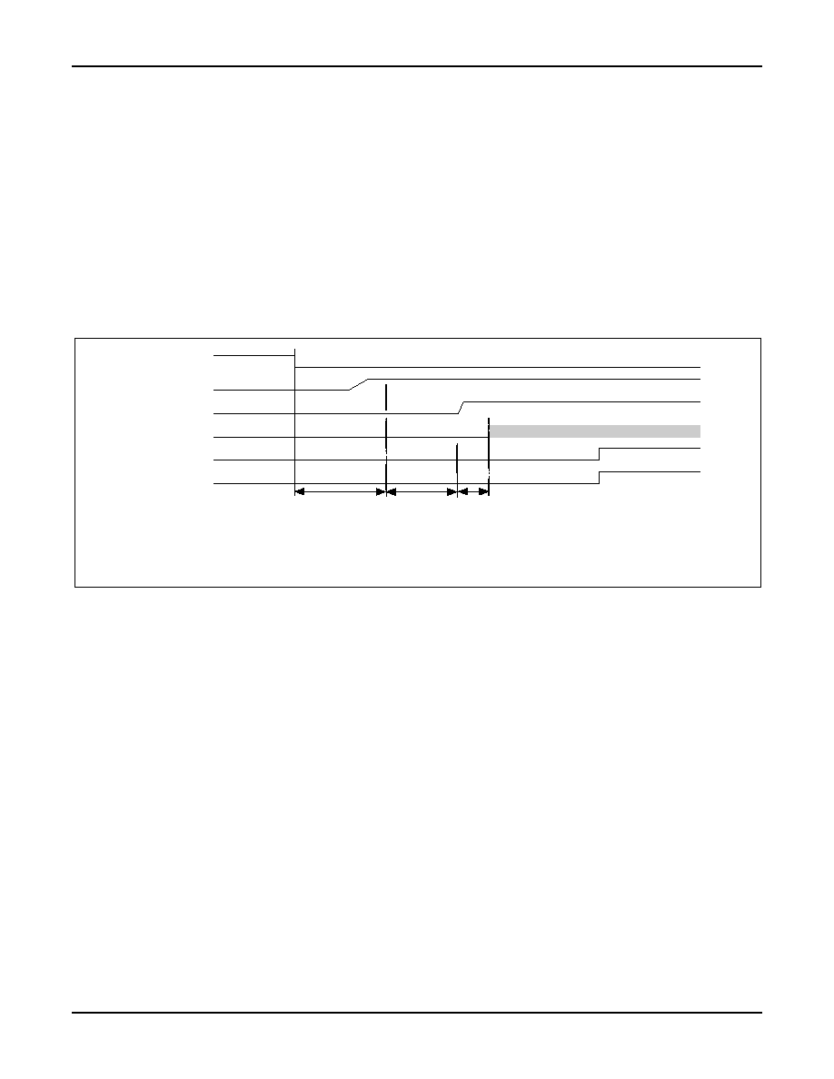
Activation Sequence
The 73S8014BN smart card interface IC has an internal 1ms delay on the application of VDD where VDD > VDDF.
No activation is allowed during this 1ms period. The
CMDVCC (edge triggered) signal must then be set low to
activate the card. To initiate activation, the card must be present and there can be no VDD fault.
The following steps show the activation sequence and the timing of the card control signals when the system
controller sets
CMDVCC low while the RSTIN is low:
CMDVCC is set low at t
0.
VCC rises to the selected level and then the internal VCC control circuit checks the presence of VCC at the
end of t1. In normal operation, the voltage VCC to the card becomes valid before t1. If VCC is not valid at t1,
OFF goes low to report a fault to the system controller, and V
CC to the card is shut off.
Turn I/O to reception mode at t2.
CLK is applied to the card at t3.
RST is a copy of RSTIN after t3.
CMDVCC
VCC
I/O
CLK
RSTIN
t1
t2
t3
RST
t0
t1 = 0.2ms (timing by 1.5MHz internal oscillator)
t2 = 1.5s, I/O goes to reception state
t3 = > 0.5s, CLK starts, RST to become the copy of RSTIN
Figure 6: Activation Sequence—RSTIN Low When
CMDVCC Goes Low
The startup of the CLK output can be delayed in the activation sequence by setting the RSTIN input high before
beginning activation by bringing
CMDVCC low. The CLK output is delayed until RSTIN is taken low. Special care
must be taken when performing this type of activation. The power-down mode is initiated by setting the RSTIN
and 5V/
3V inputs high while CMDVCC is high (outside a card session). If this state is held for more than 2ms, the
power mode is initiated. As a result, to use this activation mode, the
CMDVCC falling edge must occur within 1ms
of the RSTIN input being set high. The following steps show the activation sequence and the timing of the card
control signals when the system controller pulls the
CMDVCC low while the RSTIN is high:
CMDVCC is set low at t
0.
VCC rises to the selected level and then the internal VCC control circuit checks the presence of VCC at the
end of t1. In normal operation, the voltage VCC to the card becomes valid before t1. If VCC is not valid at t1,
OFF goes low to report a fault to the system controller, and V
CC to the card is shut off.
At the fall of RSTIN (under host control) at t2, CLK is applied to the card.
RST is a copy of RSTIN after t2.
相關PDF資料 |
PDF描述 |
|---|---|
| 73S8014BN-IL/F | SPECIALTY ANALOG CIRCUIT, PDSO20 |
| 73S8014RN-IL/F | SPECIALTY ANALOG CIRCUIT, PDSO20 |
| 73S8014RN-ILR/F | SPECIALTY ANALOG CIRCUIT, PDSO20 |
| 73S8023C-IM | SPECIALTY ANALOG CIRCUIT, QCC32 |
| 73S8023C-IM | SPECIALTY ANALOG CIRCUIT, QCC32 |
相關代理商/技術參數 |
參數描述 |
|---|---|
| 73S8014R | 制造商:TERIDIAN 制造商全稱:TERIDIAN 功能描述:Smart Card Interface |
| 73S8014R-DB | 功能描述:界面開發工具 73S8014RRN/RT Demo Brd RoHS:否 制造商:Bourns 產品:Evaluation Boards 類型:RS-485 工具用于評估:ADM3485E 接口類型:RS-485 工作電源電壓:3.3 V |
| 73S8014R-IL/F | 功能描述:I2C 接口集成電路 Smart Card Interface Comp w/8024 RoHS:否 制造商:NXP Semiconductors 電源電壓-最大:5.5 V 電源電壓-最小:2.3 V 最大工作頻率:400 KHz 最大工作溫度:+ 85 C 封裝 / 箱體:TSSOP-16 |
| 73S8014R-IL/F1 | 功能描述:輸入/輸出控制器接口集成電路 RoHS:否 制造商:Silicon Labs 產品: 輸入/輸出端數量: 工作電源電壓: 最大工作溫度:+ 85 C 最小工作溫度:- 40 C 安裝風格:SMD/SMT 封裝 / 箱體:QFN-64 封裝:Tray |
| 73S8014R-IL/F2 | 功能描述:輸入/輸出控制器接口集成電路 Smart Card Interface Comp w/8024 RoHS:否 制造商:Silicon Labs 產品: 輸入/輸出端數量: 工作電源電壓: 最大工作溫度:+ 85 C 最小工作溫度:- 40 C 安裝風格:SMD/SMT 封裝 / 箱體:QFN-64 封裝:Tray |
發布緊急采購,3分鐘左右您將得到回復。