- 您現在的位置:買賣IC網 > PDF目錄369340 > 75433-EP (Texas Instruments, Inc.) POWER GOOD FAST-TRANSIENT-RESPONSE 2-A LOW-DROPOUT VOLTAGE REGULATORS PDF資料下載
參數資料
| 型號: | 75433-EP |
| 廠商: | Texas Instruments, Inc. |
| 元件分類: | 基準電壓源/電流源 |
| 英文描述: | POWER GOOD FAST-TRANSIENT-RESPONSE 2-A LOW-DROPOUT VOLTAGE REGULATORS |
| 中文描述: | 電源良好快速瞬態響應2 -低壓差電壓調節器 |
| 文件頁數: | 25/27頁 |
| 文件大小: | 388K |
| 代理商: | 75433-EP |
第1頁第2頁第3頁第4頁第5頁第6頁第7頁第8頁第9頁第10頁第11頁第12頁第13頁第14頁第15頁第16頁第17頁第18頁第19頁第20頁第21頁第22頁第23頁第24頁當前第25頁第26頁第27頁
TPS75201-EP TPS75215-EP TPS75218-EP TPS75225-EP TPS75233-EP WITH RESET
TPS75401-EP
’
75415-EP
’
75418-EP
’
75425-EP
’
75433-EP WITH POWER GOOD
FAST-TRANSIENT-RESPONSE 2-A LOW-DROPOUT VOLTAGE REGULATORS
SGLS165
–
APRIL 2003
25
POST OFFICE BOX 655303
DALLAS, TEXAS 75265
THERMAL INFORMATION
thermally enhanced TSSOP-20 (PWP
–
PowerPad
) (continued)
If the system implements a TPS75233QPWPEP regulator, where V
I
= 5 V and I
O
= 800 mA, the internal power
dissipation is:
PD(total)
VI
VO
IO
(5
3.3)
0.8
1.36 W
(9)
Comparing P
D(total)
with P
D(max)
reveals that the power dissipation in this example does not exceed the calculated
limit. When it does, one of two corrective actions should be made: raising the power-dissipation limit by increasing
the airflow or the heat-sink area, or lowering the internal power dissipation of the regulator by reducing the input
voltage or the load current. In either case, the above calculations should be repeated with the new system
parameters.
mounting information
The primary requirement is to complete the thermal contact between the thermal pad and the PWB metal. The
thermal pad is a solderable surface and is fully intended to be soldered at the time the component is mounted.
Although voiding in the thermal-pad solder-connection is not desirable, up to 50% voiding is acceptable. The data
included in Figures 26 and 27 is for soldered connections with voiding between 20% and 50%. The thermal analysis
shows no significant difference resulting from the variation in voiding percentage.
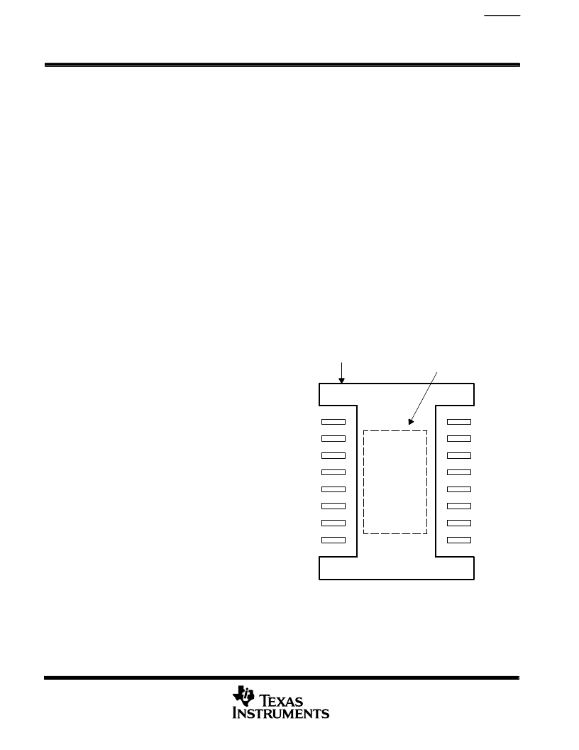
Figure 29 shows the solder-mask land pattern for the
PWP package. The minimum recommended heat-
sink area is also illustrated. This is simply a copper
plane under the body extent of the package, including
metal routed under terminals 1, 10, 11, and 20.
Figure 29. PWP Package Land Pattern
Location of Exposed
Thermal Pad on
PWP Package
Minimum Recommended
Heat-Sink Area
相關PDF資料 |
PDF描述 |
|---|---|
| 75452 | DUAL PERIPHERAL DRIVERS |
| 75460 | PERIPHERAL DRIVERS FOR HIGH-VOLTAGE HIGH-CURRENT DRIVER APPLICATIONS |
| 75464 | PERIPHERAL DRIVERS FOR HIGH-VOLTAGE HIGH-CURRENT DRIVER APPLICATIONS |
| 755332-1 | Dual Low Offset, Low Power Operational Amplifier; Package: CerDIP; No of Pins: 8; Temperature Range: Military |
| 75543-010 | OSC 3.3V 8PIN TTL/CMOS |
相關代理商/技術參數 |
參數描述 |
|---|---|
| 75434-0006 | 制造商:MOLEX 功能描述:GBX BACKPLANE 3 PAIR 25 C |
| 75434-0007 | 制造商:MOLEX 功能描述:GBX BACKPLANE 3 PAIR 25 C |
| 75434-0022 | 制造商:MOLEX 功能描述:GBX BACKPLANE 3 PAIR 25 C |
| 75434-0023 | 制造商:MOLEX 功能描述:GBX 3 PAIR 10 COLUMN OPEN BACKPLANE ASSY |
| 75434-0024 | 制造商:MOLEX 功能描述:GBX 3 PAIR BPLANE CUSTUM 25 COL OPEN END |
發布緊急采購,3分鐘左右您將得到回復。