- 您現在的位置:買賣IC網 > PDF目錄250212 > 7P12FLV262C25 (MICROSEMI CORP-PMG MICROELECTRONICS) 6M X 16 FLASH 3V PROM CARD, 250 ns, XMA68 PDF資料下載
參數資料
| 型號: | 7P12FLV262C25 |
| 廠商: | MICROSEMI CORP-PMG MICROELECTRONICS |
| 元件分類: | PROM |
| 英文描述: | 6M X 16 FLASH 3V PROM CARD, 250 ns, XMA68 |
| 封裝: | CARD-68 |
| 文件頁數: | 4/11頁 |
| 文件大小: | 409K |
| 代理商: | 7P12FLV262C25 |
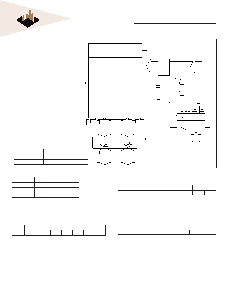
PCMCIA Flash Memory Card
FLV Series
2
White Electronic Designs Corporation (602) 437-1520 www.wedc.com
White Electronic Designs
June, 2003
Rev. 5
White Electronic Designs Corp. reserves the right to change products or specications without notice.
Device (N-2)
Device 1
CSn
Device 2
CS1
CS0
Device 3
DATA
BUS
Q0-Q7
M Res
Vcc
4000h
Device (N-1)
0000h
Card
Management
Registers
DATA
BUS
Q8-Q15
Device 0
WH#
WL#
CSn
RL#
RH#
Cn
At/Reg enable
CS0
C0
Control Logic
PCMCIA Interface
Ctrl
attrib. mem
CIS
EEPROM 2kB
SR Clr
Reg Clr
SR#
PD#
Control
Address
Bus
ADDRESS
BUFFER
Array
Address
Bus
A1-A25
Device Pair (N/2 - 1)
ADDRESS BUS
WE#
OE#
CE2#
CE1#
REG#
A0
WP
Device Pair 1
Device Pair 0
WL# RL#
RH#
WH#
Vcc
control
Q0-Q7
Vcc
I/O buffer
DATA
BUS
D0 -D7
DATA
BUS
D8 -D1 5
BLOCK DIAGRAM
ADDRESS
REGISTER NAME
4100h
Status Register
4002h
Cong. and Status Register
4000h
Conguration Option Register
REGISTERS IN ATTRIBUTE MEMORY SPACE*
COR
CONFIGURATION OPTION REGISTER: ADRS =
4000H WRITE ONLY
* FLV51- FLV58 and cards without Attribute Memory do not
have registers.
SRES
LREQ
Conguration Index
D7
D6
D5
D4
D3
D2
D1
D0
D7
Soft Reset, active High
1 = Reset State
0 = End Reset State
D6
Level Req (not supported)
D5-D0
Conguration index (not supported)
CSR
CONFIGURATION STATUS REGISTER: ADRS =
4002H WRITE ONLY
Not Supported
PDwn
Not Supported
D7
D6
D5
D4
D3
D2
D1
D0
D2
Power Down, active High
1 = Place all memory devices in power down mode
0 = Normal Operation
Power On default = 0
SR
STATUS REGISTER: ADRS = 4100H READ ONLY
Not Supported SReset
PDwn Not Supported R/BSY#
D7
D6
D5
D4
D3
D2
D1
D0
D5
Represents the state of SRESET bit in COR (4000h)
1 = Reset
0 = Normal Operation
Power On default
D5 = 0
D3
Represents the state of Power Down bit (D2) in CSR (4002h)
1 = Power Down
D0
Reects the card's Ready/Busy signal (pin 16) driven by
memory components Ready/Busy outputs. This bit allows
software polling of the card's Ready/Busy status.
1 = Ready
Device type
Manuf ID
Device ID
28F008SC
89H
A6H
28F016SC
89H
AAH
相關PDF資料 |
PDF描述 |
|---|---|
| 7P12FLV520I15 | 6M X 16 FLASH 3V PROM CARD, 150 ns, XMA68 |
| 7P24FLV251I25 | 12M X 16 FLASH 3V PROM CARD, 250 ns, XMA68 |
| 7P24FLV280I15 | 12M X 16 FLASH 3V PROM CARD, 150 ns, XMA68 |
| 7P24FLV570I25 | 12M X 16 FLASH 3V PROM CARD, 250 ns, XMA68 |
| 7203L12PDG | 2K X 9 OTHER FIFO, 12 ns, PDIP28 |
相關代理商/技術參數 |
參數描述 |
|---|---|
| 7P-12TK11C6C-BK | 制造商:Eclipse Tools 功能描述: |
| 7P14-2T12-2 | 制造商:AUGAT COMPONENTS 功能描述: |
| 7P14-2T24-2 | 制造商:AUGAT COMPONENTS 功能描述: |
| 7P14-2T36-2 | 制造商:AUGAT COMPONENTS 功能描述: |
| 7P14-2T48-2 | 制造商:AUGAT COMPONENTS 功能描述: |
發布緊急采購,3分鐘左右您將得到回復。