- 您現在的位置:買賣IC網 > PDF目錄36330 > 935089530518 (NXP SEMICONDUCTORS) SPECIALTY CONSUMER CIRCUIT, PQFP64 PDF資料下載
參數資料
| 型號: | 935089530518 |
| 廠商: | NXP SEMICONDUCTORS |
| 元件分類: | 消費家電 |
| 英文描述: | SPECIALTY CONSUMER CIRCUIT, PQFP64 |
| 封裝: | 14 X 20 MM, 2.80 MM HEIGHT, PLASTIC, SOT-319-2, QFP-64 |
| 文件頁數: | 13/47頁 |
| 文件大小: | 250K |
| 代理商: | 935089530518 |
第1頁第2頁第3頁第4頁第5頁第6頁第7頁第8頁第9頁第10頁第11頁第12頁當前第13頁第14頁第15頁第16頁第17頁第18頁第19頁第20頁第21頁第22頁第23頁第24頁第25頁第26頁第27頁第28頁第29頁第30頁第31頁第32頁第33頁第34頁第35頁第36頁第37頁第38頁第39頁第40頁第41頁第42頁第43頁第44頁第45頁第46頁第47頁
1996 Jan 26
20
Philips Semiconductors
Objective specication
I2C-bus controlled PAL/NTSC TV processors
TDA8376; TDA8376A
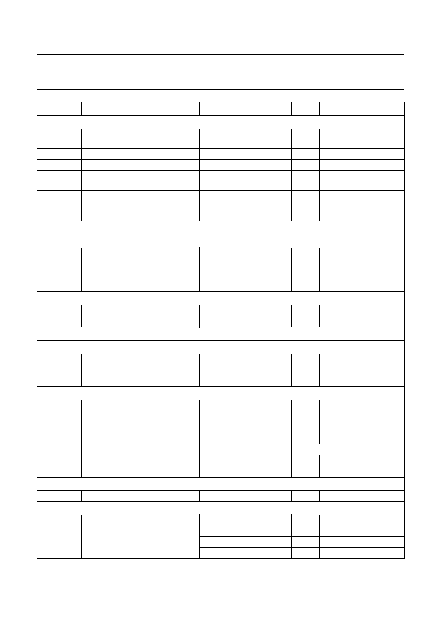
LUMINANCE INPUTS AND OUTPUTS (PINS 27 AND 28)
V28(p-p)
output signal voltage amplitude
(peak-to-peak value)
top sync to white
0.45
0.63
V
VTS
top sync voltage level
2.5
V
Zo
output impedance
250
V27(p-p)
input signal voltage amplitude
(peak-to-peak value)
0.45
V
Iclamp
clamping current during burst key
pulse
200
A
Ii
input current
no clamping
0.5
A
Chrominance lters
CHROMINANCE TRAP CIRCUIT
ftrap
trap frequency
fosc
MHz
during SECAM reception
4.2
MHz
QF
trap quality factor
note 8
2
SR
colour subcarrier rejection
20
dB
CHROMINANCE BAND-PASS CIRCUIT
fc
centre frequency
fosc
MHz
QBP
band-pass quality factor
3
Delay line, peaking circuit and black stretcher
Y DELAY LINE
td
delay time
note 2
480
ns
td1
tuning range delay time
8 steps
160
+160
ns
B
bandwidth of internal delay line
note 2
5
MHz
PEAKING CONTROL; note 9
fc(p)
peaking centre frequency
3
MHz
tW
width of preshoot or overshoot
at 50% of pulse; note 2
160
ns
OS
overshoot
positive
20
%
negative
36
%
peaking control curve
16 steps
see Fig.5
GW
wave gain
1.8
CORING STAGE
S
coring range
15
IRE
BLACK LEVEL STRETCHER (PIN 2); note 10
BLSmax
maximum black level shift
15
21
27
IRE
LSH
level shift
100% of peak-white
1
0
+1
IRE
50% of peak-white
1
+3
IRE
15% of peak-white
6
8
10
IRE
SYMBOL
PARAMETER
CONDITIONS
MIN.
TYP.
MAX.
UNIT
negative half wave gain
positive half wave gain
--------------------------------------------------------------
相關PDF資料 |
PDF描述 |
|---|---|
| 935071060157 | SPECIALTY CONSUMER CIRCUIT, PQFP80 |
| 935077580157 | SPECIALTY CONSUMER CIRCUIT, PQFP80 |
| 935206750518 | SPECIALTY CONSUMER CIRCUIT, PQFP80 |
| 935206750557 | SPECIALTY CONSUMER CIRCUIT, PQFP80 |
| 935075380112 | SPECIALTY CONSUMER CIRCUIT, PDSO28 |
相關代理商/技術參數 |
參數描述 |
|---|---|
| 9350DC-200-0GZZZA | 制造商:Siemens 功能描述: |
| 9350DC-200-0ZZZTA | 制造商:Siemens 功能描述: |
| 9350DC-200-0ZZZZA | 制造商:Siemens 功能描述: |
| 9350-DISPLAY | 制造商:Siemens 功能描述: |
| 9350SC-100-0GZZZA | 制造商:Siemens 功能描述: |
發布緊急采購,3分鐘左右您將得到回復。