- 您現(xiàn)在的位置:買賣IC網(wǎng) > PDF目錄36338 > 935262202112 (NXP SEMICONDUCTORS) VERTICAL DEFLECTION IC, PSIP9 PDF資料下載
參數(shù)資料
| 型號: | 935262202112 |
| 廠商: | NXP SEMICONDUCTORS |
| 元件分類: | 偏轉(zhuǎn) |
| 英文描述: | VERTICAL DEFLECTION IC, PSIP9 |
| 封裝: | POWER, PLASTIC, SOT-131-2, SIP-9 |
| 文件頁數(shù): | 9/14頁 |
| 文件大小: | 106K |
| 代理商: | 935262202112 |
1999 Sep 27
4
Philips Semiconductors
Product specication
DC-coupled vertical deection circuit
TDA8356
PINNING
FUNCTIONAL DESCRIPTION
The vertical driver circuit is a bridge configuration. The
deflection coil is connected between the output amplifiers,
which are driven in opposite phase. An external resistor
(RM) connected in series with the deflection coil provides
internal feedback information. The differential input circuit
is voltage driven. The input circuit has been adapted to
enable it to be used with the TDA9150, TDA9151B,
TDA9160A, TDA9162, TDA8366 and TDA8376 which
deliver symmetrical current signals. An external resistor
(RCON) connected between the differential input
determines the output current through the deflection coil.
The relationship between the differential input current and
the output current is defined by: Idiff × RCON =Icoil × RM.
The output current is adjustable from 0.5 A (p-p) to
2 A (p-p) by varying RM. The maximum input differential
voltage is 1.8 V. In the application it is recommended that
Vdiff = 1.5 V (typ). This is recommended because of the
spread of input current and the spread in the value of
RCON.
The flyback voltage is determined by an additional supply
voltage VFB. The principle of operating with two supply
voltages (class G) makes it possible to fix the supply
voltage VP optimum for the scan voltage and the second
supply voltage VFB optimum for the flyback voltage. Using
this method, very high efficiency is achieved.
The supply voltage VFB is almost totally available as
flyback voltage across the coil, this being possible due to
the absence of a decoupling capacitor (not necessary,
due to the bridge configuration). Built-in protections are:
Thermal protection
Short-circuit protection of the output pins (pins 4 and 7)
Short-circuit protection of the output pins to VP.
A guard circuit VO(guard) is provided. The guard circuit is
activated at the following conditions:
During flyback
During short-circuit of the coil and during short-circuit of
the output pins (pins 4 and 7) to VP or ground
During open loop
When the thermal protection is activated.
This signal can be used for blanking the picture tube
screen.
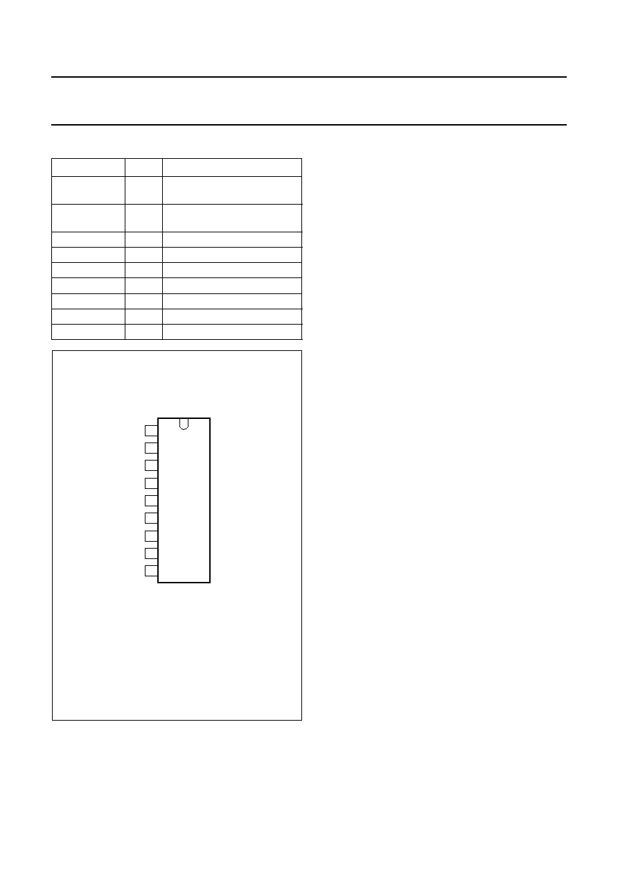
SYMBOL
PIN
DESCRIPTION
Idrive(pos)
1
input power-stage (positive);
includes II(sb) signal bias
Idrive(neg)
2
input power-stage (negative);
includes II(sb) signal bias
VP
3
operating supply voltage
VO(B)
4
output voltage B
GND
5
ground
VFB
6
input yback supply voltage
VO(A)
7
output voltage A
VO(guard)
8
guard output voltage
VI(fb)
9
input feedback voltage
Fig.2 Pin configuration.
Metal block connected to substrate pin 5.
Metal on back.
handbook, 2 columns
1
2
3
4
5
6
7
8
9
TDA8356
I drive(pos)
VI(fb)
VP
VO(B)
GND
V FB
VO(A)
VO(guard)
I drive(neg)
MGC092
相關(guān)PDF資料 |
PDF描述 |
|---|---|
| 935262254551 | 3-CH 8-BIT PROPRIETARY METHOD ADC, PARALLEL ACCESS, PQFP100 |
| 935262255557 | 3-CH 8-BIT PROPRIETARY METHOD ADC, PARALLEL ACCESS, PQFP100 |
| 935266896551 | 3-CH 8-BIT PROPRIETARY METHOD ADC, PARALLEL ACCESS, PQFP100 |
| 935266896557 | 3-CH 8-BIT PROPRIETARY METHOD ADC, PARALLEL ACCESS, PQFP100 |
| 935262255551 | 3-CH 8-BIT PROPRIETARY METHOD ADC, PARALLEL ACCESS, PQFP100 |
相關(guān)代理商/技術(shù)參數(shù) |
參數(shù)描述 |
|---|---|
| 935262217118 | 制造商:NXP Semiconductors 功能描述:Real Time Clock Serial 8-Pin SO T/R |
| 935264217557 | 制造商:NXP Semiconductors 功能描述:SUB ONLY IC |
| 935267356112 | 制造商:NXP Semiconductors 功能描述:IC TEA1507PN |
| 935268081112 | 制造商:NXP Semiconductors 功能描述:SUB ONLY IC |
| 935268721125 | 制造商:NXP Semiconductors 功能描述:Buffer/Line Driver 1-CH Non-Inverting 3-ST CMOS 5-Pin TSSOP T/R |
發(fā)布緊急采購,3分鐘左右您將得到回復(fù)。