- 您現(xiàn)在的位置:買賣IC網(wǎng) > PDF目錄36340 > 935269494115 (NXP SEMICONDUCTORS) 0.3 A SWITCHING REGULATOR, 57.5 kHz SWITCHING FREQ-MAX, PDSO5 PDF資料下載
參數(shù)資料
| 型號(hào): | 935269494115 |
| 廠商: | NXP SEMICONDUCTORS |
| 元件分類: | 穩(wěn)壓器 |
| 英文描述: | 0.3 A SWITCHING REGULATOR, 57.5 kHz SWITCHING FREQ-MAX, PDSO5 |
| 封裝: | 1.50 MM, PLASTIC, MO-178, SOT-25, SOT-23, SOP-5 |
| 文件頁(yè)數(shù): | 3/21頁(yè) |
| 文件大小: | 333K |
| 代理商: | 935269494115 |
第1頁(yè)第2頁(yè)當(dāng)前第3頁(yè)第4頁(yè)第5頁(yè)第6頁(yè)第7頁(yè)第8頁(yè)第9頁(yè)第10頁(yè)第11頁(yè)第12頁(yè)第13頁(yè)第14頁(yè)第15頁(yè)第16頁(yè)第17頁(yè)第18頁(yè)第19頁(yè)第20頁(yè)第21頁(yè)
Philips Semiconductors
Product data
SA57254-XX
CMOS switching regulator (PWM controlled)
2001 Aug 01
11
Period 1: power switch on-time
During this period, a simple circuit loop is formed when the power
switch is on. The input voltage source is connected directly across
the boost inductor (L0). A current ramp is exhibited whose slope is
described by:
IL
(
on) +
V
IN
L
0
Eqn. (1)
Energy is then stored within the core material of the inductor and is
described by:
Esto + 0.5L0
I
peak
2
Eqn. (2)
This current ramp continues until the controller turns off the power
switch.
Period 2: inductor discharge period
The instant the power switch turns off, the current flowing through
the inductor forces the voltage at its output node (switched node) to
rise quickly above the input voltage (spike). This voltage is then
clamped when it exceeds the device’s output voltage and the output
rectifier becomes forward biased. The inductor empties its stored
energy in the form of a linearly decreasing current ramp whose
slope is dictated by:
I
L(off) [
V
IN * VOUT
L
0
Eqn. (3)
The stored energy is transferred to the output capacitor. This output
current continues until the magnetic core is completely emptied of its
stored energy or the power switch turns back on.
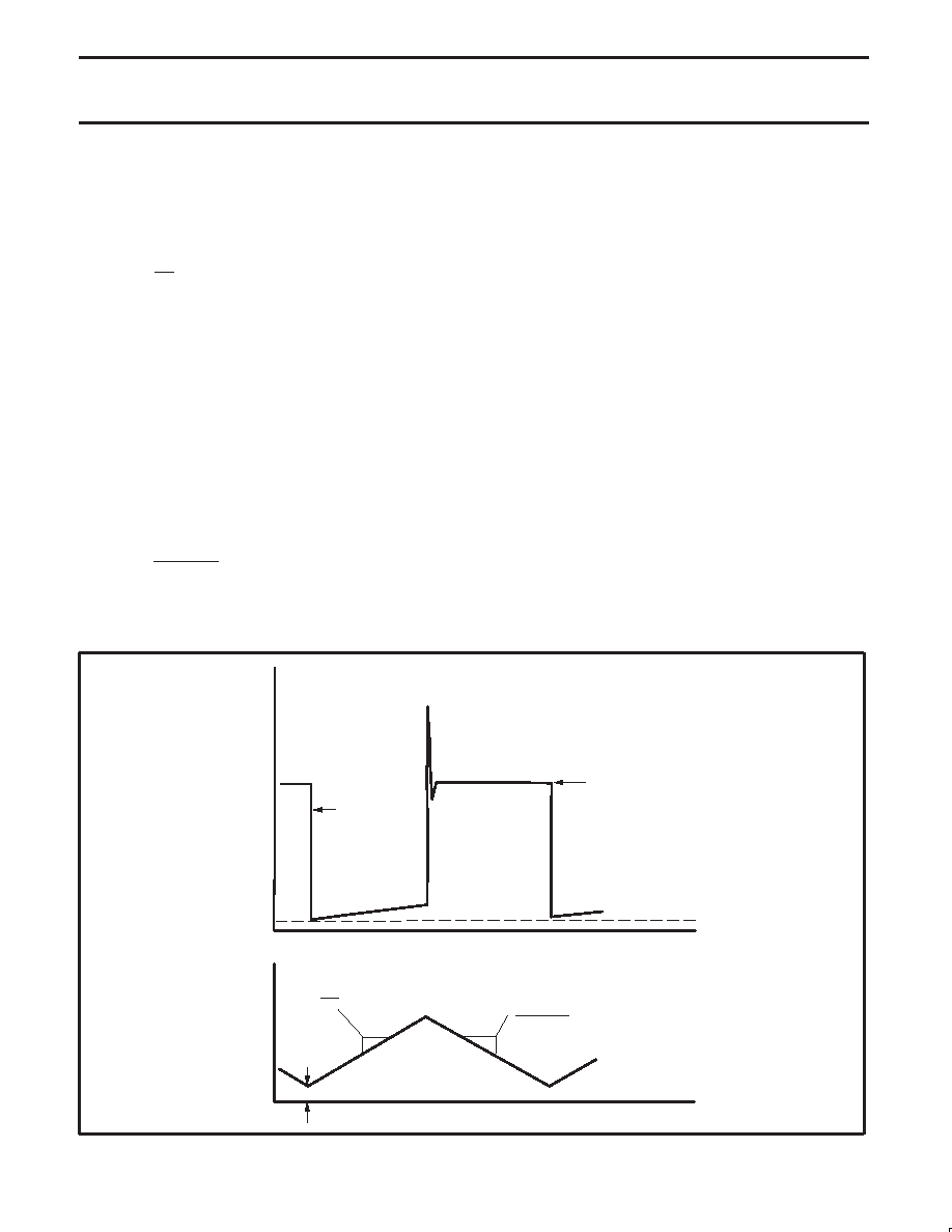
Period 3: inductor empty state
DISCONTINUOUS MODE—This period as displayed in Figure 25 occurs
in the discontinuous–mode of operation of a boost converter. It is
identified by a period of “ringing” following the output period
(period 2). The inductor has been completely emptied of its stored
energy and the switched node returns to the level of the input
voltage. Ringing is seen at this node because a resonant circuit is
formed by the inductance of L0 and any parasitic inductances and
capacitances connected to that node. This ringing has very little
energy and can easily be eliminated by a small passive snubber.
CONTINUOUS MODE—If the inductor is not completely emptied of its
stored energy before the power switch turns on again, the converter
is operating in the continuous mode. A small amount of residual flux
(energy) remains in the inductor core and the current waveform
jumps to an initial value when the power switch is again turned-on.
This mode offers some advantages over the discontinuous-mode,
because the peak current seen by the power switch is lower. In low
voltage applications, the inductor can store more energy with lower
peak currents.
The continuous mode waveforms can be seen in Figure 26.
SWITCH
VOLTAGE
(V)
INDUCTOR
CURRENT
(A)
0
SPIKE
+VOUT
+VIN
VIN
(VIN – VOUT)
Ipeak
RESIDUAL FLUX
ENERGY BEING
TRANSFERRED
TO OUTPUT
ENERGY BEING
STORED IN
INDUCTOR
SL01465
L0
Figure 26. Continuous mode waveforms.
相關(guān)PDF資料 |
PDF描述 |
|---|---|
| 935269493115 | 0.3 A SWITCHING REGULATOR, 57.5 kHz SWITCHING FREQ-MAX, PDSO5 |
| 935269492115 | 0.3 A SWITCHING REGULATOR, 57.5 kHz SWITCHING FREQ-MAX, PDSO5 |
| 935269491115 | 0.3 A SWITCHING REGULATOR, 57.5 kHz SWITCHING FREQ-MAX, PDSO5 |
| 935269496115 | 0.3 A SWITCHING REGULATOR, 57.5 kHz SWITCHING FREQ-MAX, PDSO5 |
| 935269576557 | SPECIALTY CONSUMER CIRCUIT, PQFP100 |
相關(guān)代理商/技術(shù)參數(shù) |
參數(shù)描述 |
|---|---|
| 935269544557 | 制造商:NXP Semiconductors 功能描述:SUB ONLY TDA9587-2US1-V1.3 |
| 935269987557 | 制造商:NXP Semiconductors 功能描述:SUB ONLY TDA9587-1US1-V1.8 SUBBED TO 935269987557 |
| 935270713557 | 制造商:NXP Semiconductors 功能描述:SUB ONLY IC CHP |
| 935270792551 | 制造商:NXP Semiconductors 功能描述:IC BUFF DVR TRI-ST 16BIT 56VFBGA |
| 935270792557 | 制造商:NXP Semiconductors 功能描述:IC BUFF DVR TRI-ST 16BIT 56VFBGA |
發(fā)布緊急采購(gòu),3分鐘左右您將得到回復(fù)。