- 您現在的位置:買賣IC網 > PDF目錄36340 > 935269494115 (NXP SEMICONDUCTORS) 0.3 A SWITCHING REGULATOR, 57.5 kHz SWITCHING FREQ-MAX, PDSO5 PDF資料下載
參數資料
| 型號: | 935269494115 |
| 廠商: | NXP SEMICONDUCTORS |
| 元件分類: | 穩壓器 |
| 英文描述: | 0.3 A SWITCHING REGULATOR, 57.5 kHz SWITCHING FREQ-MAX, PDSO5 |
| 封裝: | 1.50 MM, PLASTIC, MO-178, SOT-25, SOT-23, SOP-5 |
| 文件頁數: | 7/21頁 |
| 文件大小: | 333K |
| 代理商: | 935269494115 |
Philips Semiconductors
Product data
SA57254-XX
CMOS switching regulator (PWM controlled)
2001 Aug 01
15
Laying out the printed circuit board
The design of the printed circuit board (PCB) is critical to the proper
operation of all switching power supplies. Its design affects the
supply stability, radio frequency interference behavior and the
reliability of the converter.
Never use the autoroute feature of any PCB design program
because this will always produce traces that are too long and too
thin.
The input and output capacitors are the only source or sink of the
high frequency currents found in a switching power supply. All
connections to the switching power supply from the outside circuits
should be made to the input or output capacitor terminals (+ and –).
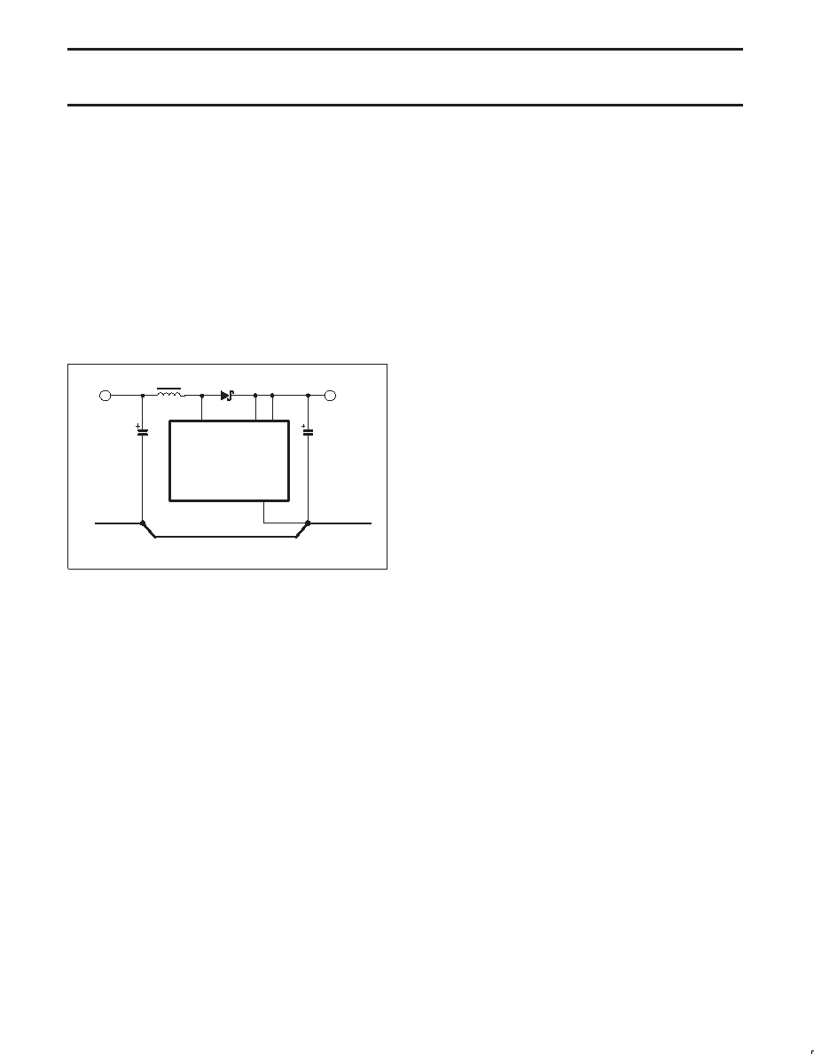
Internally, the layout should adhere to a “one-point” grounding
system, as shown in Figure 30.
SL01507
VIN
CIN
GND
SA57254-XX
SW
FB
VOUT
COUT
OUTPUT
GROUND
TO ONE POINT
INPUT
GROUND
TO ONE POINT
VDD
L0
Figure 30. Grounding trace for converter.
The traces between the input and output capacitors and the
inductor, power switch and rectifier(s) should be as short and wide
as possible. This reduces the series resistance and inductance that
can be introduced by traces.
The guidelines for a PCB layout can be summarized as:
The traces between the input and output capacitor to the inductor,
power switch and the rectifier should be made as short and as
wide as possible.
Strictly adhere to the one-point wiring practices shown in
Figure 30.
On a 2-sided board, do not run sensitive signals traces under the
AC voltage node.
The IC (control) ground is terminated at the output capacitor’s
negative terminal.
Designing the PCB for effective heat dissipation
The maximum junction temperature is +125
°C, which should not be
exceeded under any operating conditions. Designing a PCB that
includes a heatsink system under the device is the key to cooler
operation of the circuit, and the long–term reliable operation of the
converter.
The major sources of heat within the converter are the power switch
inside the SA57254-XX, the resistive losses within the inductor, and
losses associated with the output rectifier. These losses can be
estimated by the following equations:
Power switch:
P
D(sw) ^ TON
I
PK
2
R
DS(ON)
f
SW
Eqn. (11)
Inductor:
P
D(L0) ^ Ipk
2
R
winding
Eqn. (12)
Output rectifier:
P
D(rect) ^ IOUT(Vfwd)
Eqn. (13)
The thermal resistance (Rth(j-a)) of the SA57254-XX is approximately
220
°C/W, assuming the device is soldered to a 2 oz. copper FR4
fiberglass circuit board, and that the minimum footprint was used
(copper just under the leads). A rule of thumb in PCB design is that
the thermal resistance can be reduced by 30% for each doubling of
the copper area close to the device. This effect diminishes for areas
greater than five times the minimum PCB footprint. If you take
advantage of this rule, thermal resistance can be reduced by using
wide copper lands when connecting to the leads of the major
power-producing parts. These PCB traces should almost fill the
areas surrounding the converter parts to conduct heat away from
the device. For demanding applications, additional heat dissipation
area can be created by placing a copper island on the opposite side
of the PCB from each wide trace and connecting it to the trace with
vias (plated thru holes).
The junction temperature can be estimated by Equation (14).
T
j ^ (PD
R
th(j-a) ) ) Tamb(max)
Eqn. (14)
Where:
PD is the power dissipation (W).
Rth(j-a)′ is the effective thermal resistance with the additional
copper (
°C/W).
Tamb is the highest local expected ambient temperature (°C).
相關PDF資料 |
PDF描述 |
|---|---|
| 935269493115 | 0.3 A SWITCHING REGULATOR, 57.5 kHz SWITCHING FREQ-MAX, PDSO5 |
| 935269492115 | 0.3 A SWITCHING REGULATOR, 57.5 kHz SWITCHING FREQ-MAX, PDSO5 |
| 935269491115 | 0.3 A SWITCHING REGULATOR, 57.5 kHz SWITCHING FREQ-MAX, PDSO5 |
| 935269496115 | 0.3 A SWITCHING REGULATOR, 57.5 kHz SWITCHING FREQ-MAX, PDSO5 |
| 935269576557 | SPECIALTY CONSUMER CIRCUIT, PQFP100 |
相關代理商/技術參數 |
參數描述 |
|---|---|
| 935269544557 | 制造商:NXP Semiconductors 功能描述:SUB ONLY TDA9587-2US1-V1.3 |
| 935269987557 | 制造商:NXP Semiconductors 功能描述:SUB ONLY TDA9587-1US1-V1.8 SUBBED TO 935269987557 |
| 935270713557 | 制造商:NXP Semiconductors 功能描述:SUB ONLY IC CHP |
| 935270792551 | 制造商:NXP Semiconductors 功能描述:IC BUFF DVR TRI-ST 16BIT 56VFBGA |
| 935270792557 | 制造商:NXP Semiconductors 功能描述:IC BUFF DVR TRI-ST 16BIT 56VFBGA |
發布緊急采購,3分鐘左右您將得到回復。