- 您現在的位置:買賣IC網 > PDF目錄25569 > 9LPR501SGLF (INTEGRATED DEVICE TECHNOLOGY INC) SPECIALTY MICROPROCESSOR CIRCUIT, PDSO64 PDF資料下載
參數資料
| 型號: | 9LPR501SGLF |
| 廠商: | INTEGRATED DEVICE TECHNOLOGY INC |
| 元件分類: | 微控制器/微處理器 |
| 英文描述: | SPECIALTY MICROPROCESSOR CIRCUIT, PDSO64 |
| 封裝: | 6.10 MM, 0.50 MM PITCH, ROHS COMPLIANT, MO-153, TSSOP-64 |
| 文件頁數: | 1/21頁 |
| 文件大小: | 197K |
| 代理商: | 9LPR501SGLF |
ICS9LPR501
IDTTM/ICSTM
64-pin CK505 w/Fully Integrated Voltage Regulator
1118N—05/19/11
64-PIN CK505 W/FULLY INTEGRATED VOLTAGE
REGULATOR
1
Datasheet
Recommended Application:
Key Specifications:
CK505 compliant clock with fully integrated voltage
regulator, PCIe Gen 1 compliant
CPU outputs cycle-cycle jitter < 85ps
SRC output cycle-cycle jitter < 125ps
PCI outputs cycle-cycle jitter < 250ps
+/- 100ppm frequency accuracy on CPU & SRC
clocks
Pin Configuration
Output Features:
2 - CPU differential low power push-pull pairs
10 - SRC differential low power push-pull pairs
1 - CPU/SRC selectable differential low power push-pull
pair
1 - SRC/DOT selectable differential low power push-pull
pair
5 - PCI, 33MHz
1 - PCI_F, 33MHz free running
1 - USB, 48MHz
1 - REF, 14.318MHz
Features/Benefits:
Does not require external pass transistor for voltage
regulator
Supports spread spectrum modulation, default is 0.5%
down spread
Uses external 14.318MHz crystal, external crystal
load caps are required for frequency tuning
One differential push-pull pair selectable between
SRC and two single-ended outputs
PCI0/CR#_A 1
64 SCLK
VDDPCI 2
63 SDATA
PCI1/CR#_B 3
62 REF0/FSLC/TEST_SEL
PCI2/TME 4
61 VDDREF
PCI3 5
60 X1
PCI4/SRC5_EN 6
59 X2
PCI_F5/ITP_EN 7
58 GNDREF
GNDPCI 8
57 FSLB/TEST_MODE
VDD48 9
56 CK_PWRGD/PD#
USB_48MHz/FSLA 10
55 VDDCPU
GND48 11
54 CPUT0
VDD96_IO 12
53 CPUC0
DOTT_96/SRCT0 13
52 GNDCPU
DOTC_96/SRCC0 14
51 CPUT1_F
GND 15
50 CPUC1_F
VDD 16
49 VDDCPU_IO
SRCT1/SE1 17
48 NC
SRCC1/SE2 18
47 CPUT2_ITP/SRCT8
GND 19
46 CPUC2_ITP/SRCC8
VDDPLL3_IO 20
45 VDDSRC_IO
SRCT2/SATAT 21
44 SRCT7/CR#_F
SRCC2/SATAC 22
43 SRCC7/CR#_E
GNDSRC 23
42 GNDSRC
SRCT3/CR#_C 24
41 SRCT6
SRCC3/CR#_D 25
40 SRCC6
VDDSRC_IO 26
39 VDDSRC
SRCT4 27
38 PCI_STOP#/SRCT5
SRCC4 28
37 CPU_STOP#/SRCC5
GNDSRC 29
36 VDDSRC_IO
SRCT9 30
35 SRCC10
SRCC9 31
34 SRCT10
SRCC11/CR#_G 32
33 SRCT11/CR#_H
64-pin TSSOP
* Internal Pull-Up Resistor
** Internal Pull-Down Resistor
9L
P
R
5
0
1
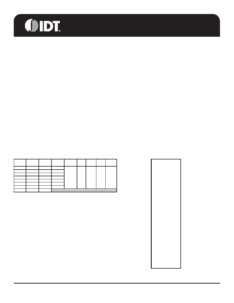
Table 1: CPU Frequency Select Table
FSLC
2
B0b7
FSLB
1
B0b6
FSLA
1
B0b5
CPU
MHz
SRC
MHz
PCI
MHz
REF
MHz
USB
MHz
DOT
MHz
00
0
266.66
00
1
133.33
01
0
200.00
01
1
166.66
10
0
333.33
10
1
100.00
11
0
400.00
11
1
1. FS
LA and FSLB are low-threshold inputs.Please see VIL_FS and VIH_FS specifications in
the Input/Supply/Common Output Parameters Table for correct values.
Also refer to the Test Clarification Table.
2. FS
LC is a three-level input. Please see the VIL_FS and VIH_FS
specifications in the Input/Supply/Common Output Parameters Table for correct values.
96.00
Reserved
100.00
33.33
14.318
48.00
相關PDF資料 |
PDF描述 |
|---|---|
| 9LPR501SGLFT | SPECIALTY MICROPROCESSOR CIRCUIT, PDSO64 |
| 9LPR501YGT | SPECIALTY MICROPROCESSOR CIRCUIT, PDSO64 |
| 9LPR502YGLFT | SPECIALTY MICROPROCESSOR CIRCUIT, PDSO56 |
| 9LPRS365BKLFT | SPECIALTY MICROPROCESSOR CIRCUIT, PQCC64 |
| 9LPRS365BGLFT | SPECIALTY MICROPROCESSOR CIRCUIT, PDSO64 |
相關代理商/技術參數 |
參數描述 |
|---|---|
| 9LPR501SGLFT | 功能描述:時鐘合成器/抖動清除器 PC MAIN CLOCK RoHS:否 制造商:Skyworks Solutions, Inc. 輸出端數量: 輸出電平: 最大輸出頻率: 輸入電平: 最大輸入頻率:6.1 GHz 電源電壓-最大:3.3 V 電源電壓-最小:2.7 V 封裝 / 箱體:TSSOP-28 封裝:Reel |
| 9LPR501YGLFT | 制造商:IDT 制造商全稱:Integrated Device Technology 功能描述:64-PIN CK505 W/FULLY INTEGRATED VOLTAGE REGULATOR |
| 9LPR502HGLF | 制造商:Integrated Device Technology Inc 功能描述:PC CLOCK, TSSOP56 - Rail/Tube |
| 9LPR502HGLFT | 制造商:Integrated Device Technology Inc 功能描述:PC CLOCK, TSSOP56 - Rail/Tube |
| 9LPR502SGLF | 功能描述:時鐘合成器/抖動清除器 PC MAIN CLOCK RoHS:否 制造商:Skyworks Solutions, Inc. 輸出端數量: 輸出電平: 最大輸出頻率: 輸入電平: 最大輸入頻率:6.1 GHz 電源電壓-最大:3.3 V 電源電壓-最小:2.7 V 封裝 / 箱體:TSSOP-28 封裝:Reel |
發布緊急采購,3分鐘左右您將得到回復。