- 您現在的位置:買賣IC網 > PDF目錄164972 > A3PN125-Z2VQG100 FPGA, 3072 CLBS, 125000 GATES, PQFP100 PDF資料下載
參數資料
| 型號: | A3PN125-Z2VQG100 |
| 元件分類: | FPGA |
| 英文描述: | FPGA, 3072 CLBS, 125000 GATES, PQFP100 |
| 封裝: | 14 X 14 MM, 1.20 MM HEIGHT, 0.50 MM PITCH, ROHS COMPLIANT, VQFP-100 |
| 文件頁數: | 60/100頁 |
| 文件大小: | 3284K |
| 代理商: | A3PN125-Z2VQG100 |
第1頁第2頁第3頁第4頁第5頁第6頁第7頁第8頁第9頁第10頁第11頁第12頁第13頁第14頁第15頁第16頁第17頁第18頁第19頁第20頁第21頁第22頁第23頁第24頁第25頁第26頁第27頁第28頁第29頁第30頁第31頁第32頁第33頁第34頁第35頁第36頁第37頁第38頁第39頁第40頁第41頁第42頁第43頁第44頁第45頁第46頁第47頁第48頁第49頁第50頁第51頁第52頁第53頁第54頁第55頁第56頁第57頁第58頁第59頁當前第60頁第61頁第62頁第63頁第64頁第65頁第66頁第67頁第68頁第69頁第70頁第71頁第72頁第73頁第74頁第75頁第76頁第77頁第78頁第79頁第80頁第81頁第82頁第83頁第84頁第85頁第86頁第87頁第88頁第89頁第90頁第91頁第92頁第93頁第94頁第95頁第96頁第97頁第98頁第99頁第100頁
ProASIC3 nano DC and Switching Characteristics
2- 48
Advance v0.2
Global Tree Timing Characteristics
Global clock delays include the central rib delay, the spine delay, and the row delay. Delays do not
include I/O input buffer clock delays, as these are I/O standard–dependent, and the clock may be
driven and conditioned internally by the CCC module. For more details on clock conditioning
capabilities, refer to the "Clock Conditioning Circuits" section on page 2-51. Table 2-63 to
Table 2-68 on page 2-50 present minimum and maximum global clock delays within each device.
Minimum and maximum delays are measured with minimum and maximum loading.
Timing Characteristics
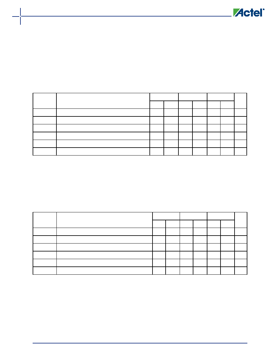
Table 2-63 A3PN010 Global Resource
Commercial-Case Conditions: TJ = 70°C, VCC = 1.425 V
Parameter Description
–2
–1
Std.
Units
Min. 1 Max. 2 Min. 1 Max. 2 Min. 1 Max. 2
tRCKL
Input LOW Delay for Global Clock
0.56
0.75
0.64
0.85
0.75
1.00
ns
tRCKH
Input HIGH Delay for Global Clock
0.57
0.79
0.65
0.90
0.76
1.05
ns
tRCKMPWH
Minimum Pulse Width HIGH for Global Clock
ns
tRCKMPWL
Minimum Pulse Width LOW for Global Clock
ns
tRCKSW
Maximum Skew for Global Clock
0.22
0.25
0.29
ns
FRMAX
Maximum Frequency for Global Clock
MHz
Notes:
1. Value reflects minimum load. The delay is measured from the CCC output to the clock pin of a sequential
element, located in a lightly loaded row (single element is connected to the global net).
2. Value reflects maximum load. The delay is measured on the clock pin of the farthest sequential element,
located in a fully loaded row (all available flip-flops are connected to the global net in the row).
3. For specific junction temperature and voltage-supply levels, refer to Table 2-6 on page 2-5 for derating
values.
Table 2-64 A3PN015 Global Resource
Commercial-Case Conditions: TJ = 70°C, VCC = 1.425 V
Parameter Description
–2
–1
Std.
Units
Min. 1 Max. 2 Min. 1 Max. 2 Min. 1 Max. 2
tRCKL
Input LOW Delay for Global Clock
0.61
0.86
0.70
0.98
0.82
1.15
ns
tRCKH
Input HIGH Delay for Global Clock
0.62
0.91
0.71
1.03
0.83
1.21
ns
tRCKMPWH
Minimum Pulse Width HIGH for Global Clock
ns
tRCKMPWL
Minimum Pulse Width LOW for Global Clock
ns
tRCKSW
Maximum Skew for Global Clock
0.28
0.32
0.38
ns
FRMAX
Maximum Frequency for Global Clock
MHz
Notes:
1. Value reflects minimum load. The delay is measured from the CCC output to the clock pin of a sequential
element, located in a lightly loaded row (single element is connected to the global net).
2. Value reflects maximum load. The delay is measured on the clock pin of the farthest sequential element,
located in a fully loaded row (all available flip-flops are connected to the global net in the row).
3. For specific junction temperature and voltage-supply levels, refer to Table 2-6 on page 2-5 for derating
values.
相關PDF資料 |
PDF描述 |
|---|---|
| A3PN125-ZVQ100I | FPGA, 3072 CLBS, 125000 GATES, PQFP100 |
| A3PN125-ZVQ100 | FPGA, 3072 CLBS, 125000 GATES, PQFP100 |
| A3PN125-ZVQG100I | FPGA, 3072 CLBS, 125000 GATES, PQFP100 |
| A3PN125-ZVQG100 | FPGA, 3072 CLBS, 125000 GATES, PQFP100 |
| A3RS91.1 | 0 MHz - 3000 MHz 50 ohm RF/MICROWAVE TERMINATION |
相關代理商/技術參數 |
參數描述 |
|---|---|
| A3PN125-Z2VQG100I | 功能描述:IC FPGA NANO 125K GATES 100-VQFP RoHS:是 類別:集成電路 (IC) >> 嵌入式 - FPGA(現場可編程門陣列) 系列:ProASIC3 nano 標準包裝:152 系列:IGLOO PLUS LAB/CLB數:- 邏輯元件/單元數:792 RAM 位總計:- 輸入/輸出數:120 門數:30000 電源電壓:1.14 V ~ 1.575 V 安裝類型:表面貼裝 工作溫度:-40°C ~ 85°C 封裝/外殼:289-TFBGA,CSBGA 供應商設備封裝:289-CSP(14x14) |
| A3PN125-ZVQ100 | 功能描述:IC FPGA NANO 125K GATES 100-VQFP RoHS:否 類別:集成電路 (IC) >> 嵌入式 - FPGA(現場可編程門陣列) 系列:ProASIC3 nano 標準包裝:152 系列:IGLOO PLUS LAB/CLB數:- 邏輯元件/單元數:792 RAM 位總計:- 輸入/輸出數:120 門數:30000 電源電壓:1.14 V ~ 1.575 V 安裝類型:表面貼裝 工作溫度:-40°C ~ 85°C 封裝/外殼:289-TFBGA,CSBGA 供應商設備封裝:289-CSP(14x14) |
| A3PN125-ZVQ100I | 功能描述:IC FPGA NANO 125K GATES 100-VQFP RoHS:否 類別:集成電路 (IC) >> 嵌入式 - FPGA(現場可編程門陣列) 系列:ProASIC3 nano 標準包裝:152 系列:IGLOO PLUS LAB/CLB數:- 邏輯元件/單元數:792 RAM 位總計:- 輸入/輸出數:120 門數:30000 電源電壓:1.14 V ~ 1.575 V 安裝類型:表面貼裝 工作溫度:-40°C ~ 85°C 封裝/外殼:289-TFBGA,CSBGA 供應商設備封裝:289-CSP(14x14) |
| A3PN125-ZVQG100 | 功能描述:IC FPGA NANO 125K GATES 100-VQFP RoHS:是 類別:集成電路 (IC) >> 嵌入式 - FPGA(現場可編程門陣列) 系列:ProASIC3 nano 標準包裝:152 系列:IGLOO PLUS LAB/CLB數:- 邏輯元件/單元數:792 RAM 位總計:- 輸入/輸出數:120 門數:30000 電源電壓:1.14 V ~ 1.575 V 安裝類型:表面貼裝 工作溫度:-40°C ~ 85°C 封裝/外殼:289-TFBGA,CSBGA 供應商設備封裝:289-CSP(14x14) |
| A3PN125-ZVQG100I | 功能描述:IC FPGA NANO 125K GATES 100-VQFP RoHS:是 類別:集成電路 (IC) >> 嵌入式 - FPGA(現場可編程門陣列) 系列:ProASIC3 nano 標準包裝:152 系列:IGLOO PLUS LAB/CLB數:- 邏輯元件/單元數:792 RAM 位總計:- 輸入/輸出數:120 門數:30000 電源電壓:1.14 V ~ 1.575 V 安裝類型:表面貼裝 工作溫度:-40°C ~ 85°C 封裝/外殼:289-TFBGA,CSBGA 供應商設備封裝:289-CSP(14x14) |
發布緊急采購,3分鐘左右您將得到回復。