- 您現(xiàn)在的位置:買賣IC網(wǎng) > PDF目錄373910 > AD760 (Analog Devices, Inc.) 16/18-Bit Self-Calibrating Serial/Byte DACPORT(16/18位自校準(zhǔn)單片D/A轉(zhuǎn)換器) PDF資料下載
參數(shù)資料
| 型號: | AD760 |
| 廠商: | Analog Devices, Inc. |
| 英文描述: | 16/18-Bit Self-Calibrating Serial/Byte DACPORT(16/18位自校準(zhǔn)單片D/A轉(zhuǎn)換器) |
| 中文描述: | 16/18-Bit自校準(zhǔn)串行/字節(jié)DACPORT(16/18位自校準(zhǔn)單片的D / A轉(zhuǎn)換器) |
| 文件頁數(shù): | 6/12頁 |
| 文件大小: | 333K |
| 代理商: | AD760 |
–6–
AD760
REV. A
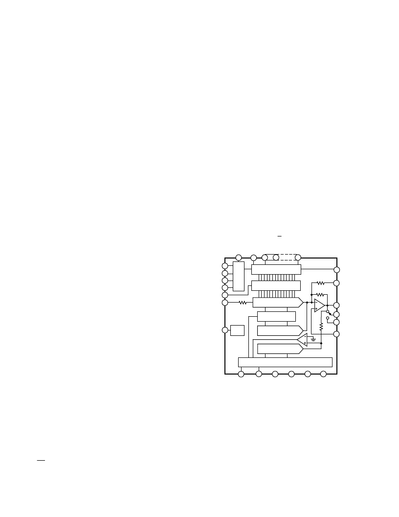
THEORY OF OPERATION
The AD760 uses autocalibration circuitry to produce a true
16-bit DAC with typically 0.2 LSB Integral and Differential
Linearity Error and 0.5 LSB Offset Error. The block diagram
in Figure 2 shows the circuit components needed for calibration.
The MAIN DAC uses an array of bipolar current sources with
MOS current steering switches to develop a current propor-
tional to the applied digital word, ranging from 0 mA to 2 mA.
A segmented architecture is used, where the most significant
four data bits are thermometer decoded to drive 15 equal cur-
rent sources. The lesser bits are scaled using an R-2R ladder,
then applied together with the segmented sources to the sum-
ming node of the output amplifier. An extra LSB is included in
the MAIN DAC, for use during calibration.
The self-calibration architecture of the AD760 attempts to
reduce the linearity errors of its transfer function. The algorithm
first checks for bipolar or unipolar operation, calibrates either
bipolar zero or unipolar offset, and then removes the carry er-
rors (DNL errors) associated with the upper 6 bits (64 codes).
Once calibrated, the top six bits of a code entering the MAIN
DAC simultaneously address the RAM, calling up a correction
code that is then applied to the CALDAC. The output cur-
rents of both the MAIN DAC and CALDAC are combined in
the summing amplifier to produce the corrected output voltage.
+10V
REF
10k
S
OUT
SPAN/
BIP
OFF
V
OUT
9.95k
LDAC
REF IN
REF OUT
HBE
SER
CLR
10k
AD760
UNI
/
BIP CLR
OR
LBE
MUX
OUT
MUX
IN
AGND
S
IN
OR
DB0
DB2
DB7
CS
MSB/
LSB
OR
DB1
12
18/16
SERIAL
OR
24
23
15
27
28
22
25
17
18
20
21
19
MAIN DAC
C
L
16
26
RAM
CALIBRATION SEQUENCER
CALOK
–V
EE
+V
CC
+V
LL
DGND
CAL
1
2
3
5
6
4
14
16/18-BIT
INPUT REGISTER
13
7
CALIBRATION DAC
16/18-BIT DAC LATCH
TRANSFER STD DAC
Figure 2. Functional Block Diagram
In the first step of DNL calibration the output of the MAIN
DAC is set to the code just below the code to be calibrated.
The extra LSB in the MAIN DAC is turned on to find the ex-
trapolated value for the next code. The comparator is then
nulled using TRANSFER STD DAC. The voltage at V
OUT
has in effect been sampled at the code to be calibrated.
Next, the extra LSB is turned off and the MAIN DAC code is
incremented by one LSB. The comparator is once again
nulled, this time with the CALDAC, until the V
OUT
is adjusted
to equal the previously sampled output. The CALDAC code is
stored in RAM and the process is repeated for the next code.
DEFINITIONS OF SPECIFICATIONS
INTEGRAL NONLINEARITY: Analog Devices defines inte-
gral nonlinearity as the maximum deviation of the actual, ad-
justed DAC output from the ideal analog output (a straight line
drawn from 0 to FS – 1 LSB) for any bit combination. This is
also referred to as relative accuracy.
DIFFERENTIAL NONLINEARITY: Differential nonlinearity
is the measure of the change in the analog output, normalized to
full scale, associated with a 1 LSB change in the digital input
code. Monotonic behavior requires that the differential linearity
error be greater than or equal to –1 LSB over the temperature
range of interest.
MONOTONICITY: A DAC is monotonic if the output either
increases or remains constant for increasing digital inputs with
the result that the output will always be a single-valued function
of the input.
GAIN ERROR: Gain error is a measure of the output error be-
tween an ideal DAC and the actual device output with all 1s
loaded after offset error has been adjusted out.
OFFSET ERROR: Offset error is a combination of the offset
errors of the voltage-mode DAC and the output amplifier and is
measured with all 0s loaded in the DAC.
BIPOLAR ZERO ERROR: When the AD760 is connected for
bipolar output and 10 . . . 000 is loaded in the DAC, the devia-
tion of the analog output from the ideal midscale value of 0 V is
called the bipolar zero error.
DRIFT: Drift is the change in a parameter (such as gain, offset
and bipolar zero) over a specified temperature range. The drift
temperature coefficient, specified in ppm/°C, is calculated by
measuring the parameter at T
MIN
, 25°C and T
MAX
and dividing
the change in the parameter by the corresponding temperature
change.
TOTAL HARMONIC DISTORTION + NOISE: Total har-
monic distortion + noise (THD+N) is defined as the ratio of the
square root of the sum of the squares of the values of the har-
monics and noise to the value of the fundamental input fre-
quency. It is usually expressed in percent (%). THD+N is a
measure of the magnitude and distribution of linearity error, dif-
ferential linearity error, quantization error and noise. The distri-
bution of these errors may be different, depending upon the
amplitude of the output signal. Therefore, to be the most useful,
THD+N should be specified for both large and small signal am-
plitudes.
SIGNAL-TO-NOISE RATIO: The signal-to-noise ratio is
defined as the ratio of the amplitude of the output when a full-
scale signal is present to the output with no signal present. This
is measured in dB.
DIGITAL-TO-ANALOG GLITCH IMPULSE: This is the
amount of charge injected from the digital inputs to the analog
output when the inputs change state. This is measured at half
scale when the DAC switches around the MSB and as many as
possible switches change state, i.e., from 011 . . . 111 to
100 . . . 000.
DIGITAL FEEDTHROUGH: When the DAC is not selected
(i.e.,
CS
is held high), high frequency logic activity on the digi-
tal inputs is capacitively coupled through the device to show up
as noise on the V
OUT
pin. This noise is digital feedthrough.
相關(guān)PDF資料 |
PDF描述 |
|---|---|
| AD7610BCPZ1 | 16-Bit, 250 kSPS, Unipolar/Bipolar Programmable Input PulSAR ADC |
| AD7610BCPZ-RL | 16-Bit, 250 kSPS, Unipolar/Bipolar Programmable Input PulSAR ADC |
| AD7610BSTZ | 16-Bit, 250 kSPS, Unipolar/Bipolar Programmable Input PulSAR ADC |
| AD7610BSTZ-RL | 16-Bit, 250 kSPS, Unipolar/Bipolar Programmable Input PulSAR ADC |
| AD7621 | 16-Bit, 1 LSB INL, 3 MSPS PulSAR ADC |
相關(guān)代理商/技術(shù)參數(shù) |
參數(shù)描述 |
|---|---|
| AD7605-4BSTZ | 功能描述:16 Bit Analog to Digital Converter 4 Input 1 SAR 64-LQFP (12x12) 制造商:analog devices inc. 系列:- 包裝:托盤 零件狀態(tài):在售 位數(shù):16 采樣率(每秒):300k 輸入數(shù):4 輸入類型:單端 數(shù)據(jù)接口:并聯(lián),SPI 配置:S/H-MUX-ADC 無線電 - S/H:ADC:1:1 A/D 轉(zhuǎn)換器數(shù):1 架構(gòu):SAR 參考類型:外部, 內(nèi)部 電壓 - 電源,模擬:5V 電壓 - 電源,數(shù)字:2.3 V ~ 5.25 V 特性:同步采樣 工作溫度:-40°C ~ 85°C 封裝/外殼:64-LQFP 供應(yīng)商器件封裝:64-LQFP(12x12) 標(biāo)準(zhǔn)包裝:1 |
| AD7605-4BSTZ-RL | 功能描述:IC ADC 16BIT 300KSPS ST642 制造商:analog devices inc. 系列:- 包裝:帶卷(TR) 零件狀態(tài):在售 位數(shù):16 采樣率(每秒):300k 輸入數(shù):4 輸入類型:單端 數(shù)據(jù)接口:并聯(lián),SPI 配置:S/H-MUX-ADC 無線電 - S/H:ADC:1:1 A/D 轉(zhuǎn)換器數(shù):1 架構(gòu):SAR 參考類型:外部, 內(nèi)部 電壓 - 電源,模擬:5V 電壓 - 電源,數(shù)字:2.3 V ~ 5.25 V 特性:同步采樣 工作溫度:-40°C ~ 85°C 封裝/外殼:64-LQFP 供應(yīng)商器件封裝:64-LQFP(12x12) 標(biāo)準(zhǔn)包裝:1,500 |
| AD7606 | 制造商:Analog Devices 功能描述:- Rail/Tube |
| AD7606-4 | 制造商:AD 制造商全稱:Analog Devices 功能描述:8-/6-/4-Channel DAS with 16-Bit,Bipolar Input,Simultaneous Sampling ADC |
| AD7606-6 | 制造商:AD 制造商全稱:Analog Devices 功能描述:8-/6-/4-Channel DAS with 16-Bit,Bipolar Input,Simultaneous Sampling ADC |
發(fā)布緊急采購,3分鐘左右您將得到回復(fù)。