- 您現在的位置:買賣IC網 > PDF目錄373911 > AD7664 (Analog Devices, Inc.) Circular Connector; No. of Contacts:4; Series:D38999; Body Material:Metal; Connecting Termination:Crimp; Connector Shell Size:13; Circular Contact Gender:Socket; Circular Shell Style:Straight Plug; Insert Arrangement:13-4 PDF資料下載
參數資料
| 型號: | AD7664 |
| 廠商: | Analog Devices, Inc. |
| 元件分類: | 圓形連接器 |
| 英文描述: | Circular Connector; No. of Contacts:4; Series:D38999; Body Material:Metal; Connecting Termination:Crimp; Connector Shell Size:13; Circular Contact Gender:Socket; Circular Shell Style:Straight Plug; Insert Arrangement:13-4 |
| 中文描述: | 16位,570 kSPS的的CMOS模數轉換器 |
| 文件頁數: | 14/19頁 |
| 文件大小: | 392K |
| 代理商: | AD7664 |
REV. 0
AD7664
–14–
DIGITAL INTERFACE
The AD7664 has a versatile digital interface; it can be interfaced
with the host system by using either a serial or parallel interface.
The serial interface is multiplexed on the parallel data bus. The
AD7664 digital interface also accommodates both 3 V or 5 V logic
by simply connecting the OVDD supply pin of the AD7664 to
the host system interface digital supply. Finally, by using the
OB/
2C
input pin, both two’s complement or straight binary
coding can be used.
The two signals
CS
and
RD
control the interface.
CS
and
RD
have a similar effect because they are OR’d together internally.
When at least one of these signals is high, the interface outputs
are in high impedance. Usually,
CS
allows the selection of each
AD7664 in multicircuits applications and is held low in a single
AD7664 design.
RD
is generally used to enable the conversion
result on the data bus.
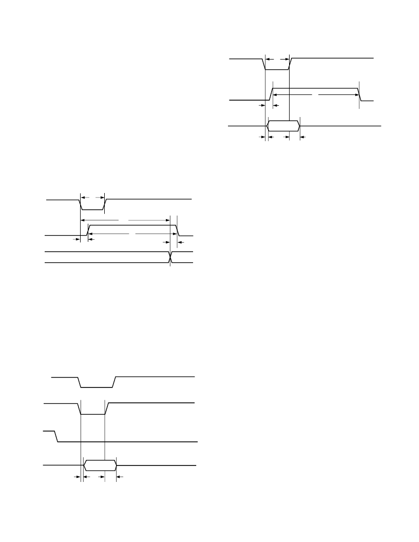
t
1
t
3
t
4
t
11
CNVST
BUSY
DATA
BUS
CS
=
RD
= 0
t
10
PREVIOUS CONVERSION DATA
NEW DATA
Figure 13. Master Parallel Data Timing for Reading
(Continuous Read)
PARALLEL INTERFACE
The AD7664 is configured to use the parallel interface when the
SER/
PAR
is held low. The data can be read either after each
conversion, which is during the next acquisition phase, or dur-
ing the following conversion as shown, respectively, in Figure 14
and Figure 15. When the data is read during the conversion,
however, it is recommended that it is read only during the first
half of the conversion phase. That avoids any potential feed-
through between voltage transients on the digital interface and
the most critical analog conversion circuitry.
CURRENT
CONVERSION
BUSY
DATA
BUS
CS
RD
t
12
t
13
Figure 14. Slave Parallel Data Timing for Reading
(Read After Convert)
PREVIOUS
CONVERSION
t
1
t
3
t
12
t
13
t
4
CS
= 0
CNVST
,
RD
BUSY
DATA
BUS
Figure 15. Slave Parallel Data Timing for Reading
(Read During Convert)
SERIAL INTERFACE
The AD7664 is configured to use the serial interface when the
SER/
PAR
is held high. The AD7664 outputs 16 bits of data,
MSB first, on the SDOUT pin. This data is synchronized with
the 16 clock pulses provided on SCLK pin. The output data is
valid on both the rising and falling edge of the data clock.
MASTER SERIAL INTERFACE
Internal Clock
The AD7664 is configured to generate and provide the serial data
clock SCLK when the EXT/
INT
pin is held low. The AD7664
also generates a SYNC signal to indicate to the host when the
serial data is valid. The serial clock SCLK and the SYNC signal
can be inverted if desired. Depending on RDC/SDIN input, the
data can be read after each conversion or during the following
conversion. Figure 16 and Figure 17 show the detailed timing
diagrams of these two modes.
Usually, because the AD7664 is used with a fast throughput, the
mode master, read during conversion is the most recommended
serial mode when it can be used.
In read-during-conversion mode, the serial clock and data toggle
at appropriate instants which minimize potential feedthrough
between digital activity and the critical conversion decisions.
In read-after-conversion mode, it should be noted that, unlike in
other modes, the signal BUSY returns low after the 16 data bits
are pulsed out and not at the end of the conversion phase which
results in a longer BUSY width.
SLAVE SERIAL INTERFACE
External Clock
The AD7664 is configured to accept an externally supplied
serial data clock on the SCLK pin when the EXT/
INT
pin is
held high. In this mode, several methods can be used to read the
data. When
CS
and
RD
are both low, the data can be read after
each conversion or during the following conversion. The exter-
nal clock can be either a continuous or discontinuous clock. A
discontinuous clock can be either normally high or normally low
when inactive. Figure 18 and Figure 20 show the detailed tim-
ing diagrams of these methods.
相關PDF資料 |
PDF描述 |
|---|---|
| AD7664ASTRL | 16-Bit, 570 kSPS CMOS ADC |
| AD7664AST | 16-Bit, 570 kSPS CMOS ADC |
| AD7665 | TV 8C 8#20 PIN PLUG |
| AD7665AST | 16-Bit, 570 kSPS CMOS ADC |
| AD7665ASTRL | 16-Bit, 570 kSPS CMOS ADC |
相關代理商/技術參數 |
參數描述 |
|---|---|
| AD7664ACP | 制造商:Analog Devices 功能描述:ADC Single SAR 570ksps 16-bit Parallel/Serial 48-Pin LFCSP EP 制造商:Analog Devices 功能描述:ADC SGL SAR 570KSPS 16BIT PARALLEL/SERL 48LFCSP EP - Trays 制造商:Rochester Electronics LLC 功能描述:16-BIT, 500KSPS CMOS ADC - Bulk |
| AD7664ACPRL | 制造商:Analog Devices 功能描述:ADC Single SAR 570ksps 16-bit Parallel/Serial 48-Pin LFCSP EP T/R |
| AD7664ACPZ | 功能描述:IC ADC 16BIT UNIPOLAR 48-LFCSP RoHS:是 類別:集成電路 (IC) >> 數據采集 - 模數轉換器 系列:PulSAR® 其它有關文件:TSA1204 View All Specifications 標準包裝:1 系列:- 位數:12 采樣率(每秒):20M 數據接口:并聯 轉換器數目:2 功率耗散(最大):155mW 電壓電源:模擬和數字 工作溫度:-40°C ~ 85°C 安裝類型:表面貼裝 封裝/外殼:48-TQFP 供應商設備封裝:48-TQFP(7x7) 包裝:Digi-Reel® 輸入數目和類型:4 個單端,單極;2 個差分,單極 產品目錄頁面:1156 (CN2011-ZH PDF) 其它名稱:497-5435-6 |
| AD7664ACPZRL | 制造商:Analog Devices 功能描述:ADC Single SAR 570ksps 16-bit Parallel/Serial 48-Pin LFCSP EP T/R 制造商:Analog Devices 功能描述:ADC SGL SAR 570KSPS 16BIT PARALLEL/SERL 48LFCSP EP - Tape and Reel |
| AD7664AST | 制造商:Analog Devices 功能描述:ADC Single SAR 570ksps 16-bit Parallel/Serial 48-Pin LQFP 制造商:Rochester Electronics LLC 功能描述:16-BIT, 500KSPS CMOS ADC - Tape and Reel 制造商:Analog Devices 功能描述:IC 16-BIT ADC |
發布緊急采購,3分鐘左右您將得到回復。