- 您現在的位置:買賣IC網 > PDF目錄373912 > AD7665AST (ANALOG DEVICES INC) 16-Bit, 570 kSPS CMOS ADC PDF資料下載
參數資料
| 型號: | AD7665AST |
| 廠商: | ANALOG DEVICES INC |
| 元件分類: | ADC |
| 英文描述: | 16-Bit, 570 kSPS CMOS ADC |
| 中文描述: | 4-CH 16-BIT SUCCESSIVE APPROXIMATION ADC, SERIAL/PARALLEL ACCESS, PQFP48 |
| 封裝: | LOW PROFILE, MS-026BBC, QFP-48 |
| 文件頁數: | 20/24頁 |
| 文件大小: | 348K |
| 代理商: | AD7665AST |
REV. 0
AD7665
–20–
CNVST
SDOUT
SCLK
D1
D0
X
D15
D14
D13
1
2
3
14
15
16
t
3
t
35
t
36
t
37
t
31
t
32
t
16
BUSY
INVSCLK = 0
CS
,
RD
EXT/
INT
= 1
RD
= 0
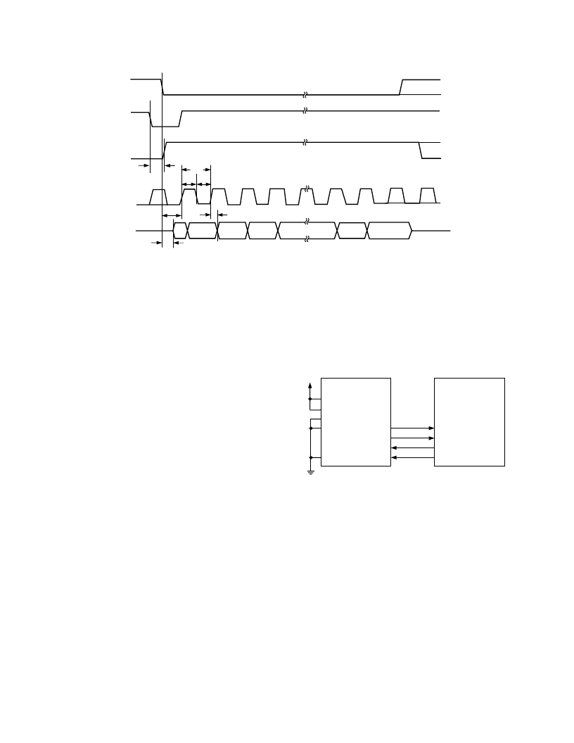
Figure 21. Slave Serial Data Timing for Reading (Read Previous Conversion During Convert)
External Clock Data Read During Conversion
Figure 21 shows the detailed timing diagrams of this method.
During a conversion, while both
CS
and
RD
are low, the result
of the previous conversion can be read. The data is shifted out,
MSB first, with 16 clock pulses and is valid on both rising and
falling edge of the clock. The 16 bits have to be read before the
current conversion is complete. If that is not done, RDERROR
is pulsed high and can be used to interrupt the host interface to
prevent incomplete data reading. There is no “daisy chain” fea-
ture in this mode and RDC/SDIN input should always be tied
either high or low.
To reduce performance degradation due to digital activity, a fast
discontinuous clock of, at least 25 MHz, when impulse mode is
used, 40 MHz when normal or warp mode is used, is recom-
mended to ensure that all the bits are read during the first half
of the conversion phase. It is also possible to begin to read the
data after conversion and continue to read the last bits even after
a new conversion has been initiated. That allows the use of a slower
clock speed like 10 MHz in impulse mode, 12 MHz in normal
mode and 15 MHz in warp mode.
MICROPROCESSOR INTERFACING
The AD7665 is ideally suited for traditional dc measurement
applications supporting a microprocessor, and ac signal process-
ing applications interfacing to a digital signal processor. The
AD7665 is designed to interface either with a parallel 8-bit or
16-bit wide interface or with a general purpose serial port or I/O
ports on a microcontroller. A variety of external buffers can be
used with the AD7665 to prevent digital noise from coupling
into the ADC. The following sections illustrate the use of the
AD7665 with an SPI equipped microcontroller, the ADSP-
21065L and ADSP-218x signal processors.
SPI Interface (MC68HC11)
Figure 22 shows an interface diagram between the AD7665 and
an SPI-equipped microcontroller like the MC68HC11. To
accommodate the slower speed of the microcontroller, the
AD7665 acts as a slave device and data must be read after con-
version. This mode also allows the “daisy chain” feature. The
convert command could be initiated in response to an internal
timer interrupt. The reading of output data, one byte at a time,
if necessary, could be initiated in response to the end-of-conver-
sion signal (BUSY going low) using an interrupt line of the
microcontroller. The Serial Peripheral Interface (SPI) on the
MC68HC11 is configured for master mode (MSTR) = 1, Clock
Polarity Bit (CPOL) = 0, Clock Phase Bit (CPHA) = 1 and SPI
interrupt enable (SPIE) = 1 by writing to the SPI Control Regis-
ter (SPCR). The IRQ is configured for edge-sensitive-only
operation (IRQE = 1 in OPTION register).
IRQ
MC68HC11
*
CNVST
AD7665
*
BUSY
CS
RD
MISO/SDI
SCK
I/O PORT
SDOUT
SCLK
INVSCLK
EXT/
INT
DVDD
*
ADDITIONAL PINS OMITTED FOR CLARITY
SER/
PAR
Figure 22. Interfacing the AD7665 to SPI Interface
ADSP-21065L in Master Serial Interface
As shown in Figure 23, the AD7665 can be interfaced to the
ADSP-21065L using the serial interface in master mode without
any glue logic required. This mode combines the advantages
of reducing the wire connections and the ability to read the
data during or after conversion maximum speed transfer
(DIVSCLK[0:1] both low).
The AD7665 is configured for the internal clock mode (EXT/
INT
low) and acts, therefore, as the master device. The convert
command can be generated by either an external low jitter oscil-
lator or, as shown, by a FLAG output of the ADSP-21065L or
by a frame output TFS of one serial port of the ADSP-21065L
which can be used like a timer. The serial port on the ADSP-
21065L is configured for external clock (IRFS = 0), rising edge
active (CKRE = 1), external late framed sync signals (IRFS = 0,
LAFS = 1, RFSR = 1) and active high (LRFS = 0). The serial
port of the ADSP-21065L is configured by writing to its receive
control register (SRCTL)—see
ADSP-2106x SHARC User’s
Manual
. Because the serial port within the ADSP-21065L will
相關PDF資料 |
PDF描述 |
|---|---|
| AD7665ASTRL | 16-Bit, 570 kSPS CMOS ADC |
| AD7669AN | LC2MOS Complete, 8-Bit Analog I/0 Systems |
| AD7569TE | LC2MOS Complete, 8-Bit Analog I/0 Systems |
| AD7569KN | LC2MOS Complete, 8-Bit Analog I/0 Systems |
| AD7569KP | LC2MOS Complete, 8-Bit Analog I/0 Systems |
相關代理商/技術參數 |
參數描述 |
|---|---|
| ad7665astrl | 制造商:Analog Devices 功能描述:ADC SGL SAR 570KSPS 16BIT PARALLEL/SERL 48LQFP - Tape and Reel 制造商:Rochester Electronics LLC 功能描述:16-BIT, 500 KSPS CMOS A/D CONVERTER - Tape and Reel |
| AD7665ASTZ | 功能描述:IC ADC 16BIT CMOS 5V 48-LQFP RoHS:是 類別:集成電路 (IC) >> 數據采集 - 模數轉換器 系列:PulSAR® 標準包裝:1 系列:- 位數:14 采樣率(每秒):83k 數據接口:串行,并聯 轉換器數目:1 功率耗散(最大):95mW 電壓電源:雙 ± 工作溫度:0°C ~ 70°C 安裝類型:通孔 封裝/外殼:28-DIP(0.600",15.24mm) 供應商設備封裝:28-PDIP 包裝:管件 輸入數目和類型:1 個單端,雙極 |
| AD7665ASTZ | 制造商:Analog Devices 功能描述:A/D Converter (A-D) IC |
| AD7665ASTZRL | 功能描述:IC ADC 16BIT CMOS 5V 48-LQFP RoHS:是 類別:集成電路 (IC) >> 數據采集 - 模數轉換器 系列:PulSAR® 標準包裝:1 系列:microPOWER™ 位數:8 采樣率(每秒):1M 數據接口:串行,SPI? 轉換器數目:1 功率耗散(最大):- 電壓電源:模擬和數字 工作溫度:-40°C ~ 125°C 安裝類型:表面貼裝 封裝/外殼:24-VFQFN 裸露焊盤 供應商設備封裝:24-VQFN 裸露焊盤(4x4) 包裝:Digi-Reel® 輸入數目和類型:8 個單端,單極 產品目錄頁面:892 (CN2011-ZH PDF) 其它名稱:296-25851-6 |
| AD7666 | 制造商:AD 制造商全稱:Analog Devices 功能描述:16-Bit 1 MSPS SAR Unipolar ADC with Ref |
發布緊急采購,3分鐘左右您將得到回復。