- 您現在的位置:買賣IC網 > PDF目錄373913 > AD7677AST (ANALOG DEVICES INC) 16-Bit, 1 LSB INL, 1 MSPS Differential ADC PDF資料下載
參數資料
| 型號: | AD7677AST |
| 廠商: | ANALOG DEVICES INC |
| 元件分類: | ADC |
| 英文描述: | 16-Bit, 1 LSB INL, 1 MSPS Differential ADC |
| 中文描述: | 1-CH 16-BIT SUCCESSIVE APPROXIMATION ADC, SERIAL/PARALLEL ACCESS, PQFP48 |
| 封裝: | LQFP-48 |
| 文件頁數: | 17/20頁 |
| 文件大小: | 322K |
| 代理商: | AD7677AST |
REV. 0
AD7677
–17–
rising and falling edge of the data clock. Depending on RDC/
SDIN input, the data can be read after each conversion, or during
the following conversion.
Figure 17 and Figure 18 show the detailed timing diagrams of
these two modes.
Usually, because the AD7677 is used with a fast throughput, the
mode master, read during conversion, is the most recommended
serial mode when it can be used.
In read-after-conversion mode, it should be noted that, unlike in
other modes, the signal BUSY returns low after the 16 data bits
are pulsed out and not at the end of the conversion phase which
results in a longer BUSY width.
In read-during-conversion mode, the serial clock and data toggle at
appropriate instances minimizes potential feedthrough between
digital activity and the critical conversion decisions.
To accommodate slow digital hosts, the serial clock can be
slowed down by using DIVSCLK.
SLAVE SERIAL INTERFACE
External Clock
The AD7677 is configured to accept an externally supplied serial
data clock on the SCLK pin when the EXT/
INT
pin is held
high. In this mode, several methods can be used to read the
data. The external serial clock is gated by
CS
and the data are
output when both
CS
and
RD
are low. Thus, depending on
CS
,
the data can be read after each conversion or during the follow-
ing conversion. The external clock can be either a continuous
or discontinuous clock. A discontinuous clock can be either
normally high or normally low when inactive. Figure 19 and
Figure 20 show the detailed timing diagrams of these methods.
While the AD7677 is performing a bit decision, it is important that
voltage transients not occur on digital input/output pins or degra-
dation of the conversion result could occur. This is particularly
important during the second half of the conversion phase because
the AD7677 provides error correction circuitry that can correct for
CS
SCLK
SDOUT
D15
D14
D1
D0
D13
X15
X14
X13
X1
X0
Y15
Y14
BUSY
SDIN
INVSCLK = 0
X15
X14
X
1
2
3
14
15
16
17
18
EXT/
INT
= 1
RD
= 0
t
35
t
36
t
37
t
31
t
32
t
34
t
16
t
33
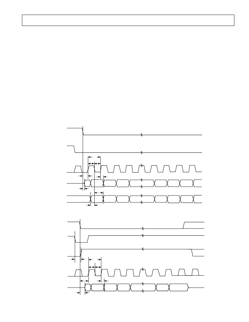
Figure 19. Slave Serial Data Timing for Reading (Read After Convert)
CNVST
SDOUT
SCLK
D1
D0
X
D15
D14
D13
1
2
3
14
15
16
BUSY
INVSCLK = 0
CS
EXT/
INT
= 1
RD
= 0
t
35
t
36
t
37
t
31
t
32
t
16
t
3
Figure 20. Slave Serial Data Timing for Reading (Read Previous Conversion During Convert)
相關PDF資料 |
PDF描述 |
|---|---|
| AD7677ASTRL | 16-Bit, 1 LSB INL, 1 MSPS Differential ADC |
| AD7679CB1 | 18-Bit, 2.5 LSB INL, 570 kSPS SAR ADC |
| AD7694 | 16-Bit, 250 kSPS PulSAR ADC in MSOP |
| AD7694ARM | 16-Bit, 250 kSPS PulSAR ADC in MSOP |
| AD7694ARMRL7 | 16-Bit, 250 kSPS PulSAR ADC in MSOP |
相關代理商/技術參數 |
參數描述 |
|---|---|
| AD7677ASTRL | 制造商:Analog Devices 功能描述:ADC Single SAR 1Msps 16-bit Parallel/Serial 48-Pin LQFP T/R |
| AD7677ASTZ | 功能描述:IC ADC 16BIT 1MSPS DIFF 48-LQFP RoHS:是 類別:集成電路 (IC) >> 數據采集 - 模數轉換器 系列:PulSAR® 標準包裝:1 系列:microPOWER™ 位數:8 采樣率(每秒):1M 數據接口:串行,SPI? 轉換器數目:1 功率耗散(最大):- 電壓電源:模擬和數字 工作溫度:-40°C ~ 125°C 安裝類型:表面貼裝 封裝/外殼:24-VFQFN 裸露焊盤 供應商設備封裝:24-VQFN 裸露焊盤(4x4) 包裝:Digi-Reel® 輸入數目和類型:8 個單端,單極 產品目錄頁面:892 (CN2011-ZH PDF) 其它名稱:296-25851-6 |
| AD7677ASTZ | 制造商:Analog Devices 功能描述:IC 16-BIT ADC |
| AD7677ASTZRL | 功能描述:IC ADC 16BIT 1MSPS DIFF 48-LQFP RoHS:是 類別:集成電路 (IC) >> 數據采集 - 模數轉換器 系列:PulSAR® 標準包裝:1 系列:- 位數:14 采樣率(每秒):83k 數據接口:串行,并聯 轉換器數目:1 功率耗散(最大):95mW 電壓電源:雙 ± 工作溫度:0°C ~ 70°C 安裝類型:通孔 封裝/外殼:28-DIP(0.600",15.24mm) 供應商設備封裝:28-PDIP 包裝:管件 輸入數目和類型:1 個單端,雙極 |
| AD7678 | 制造商:AD 制造商全稱:Analog Devices 功能描述:18-Bit, 2.5 LSB INL, 570 kSPS SAR ADC |
發布緊急采購,3分鐘左右您將得到回復。