- 您現(xiàn)在的位置:買賣IC網(wǎng) > PDF目錄373927 > AD7683ARM (ANALOG DEVICES INC) 16-Bit, 100 kSPS PulSAR ADC in MSOP/QFN PDF資料下載
參數(shù)資料
| 型號(hào): | AD7683ARM |
| 廠商: | ANALOG DEVICES INC |
| 元件分類: | ADC |
| 英文描述: | 16-Bit, 100 kSPS PulSAR ADC in MSOP/QFN |
| 中文描述: | 1-CH 16-BIT SUCCESSIVE APPROXIMATION ADC, SERIAL ACCESS, PDSO8 |
| 封裝: | MO-187AA, MSOP-8 |
| 文件頁數(shù): | 11/20頁 |
| 文件大小: | 480K |
| 代理商: | AD7683ARM |
AD7940
CIRCUIT INFORMATION
The AD7940 is a fast, low power, 14-bit, single-supply ADC. The
part can be operated from a 2.50 V to 5.5 V supply. When operated
at either 5 V or 3 V supply, the AD7940 is capable of throughput
rates of 100 kSPS when provided with a 2.5 MHz clock.
Rev. 0 | Page 11 of 20
The AD7940 provides the user with an on-chip track-and-hold
ADC and a serial interface housed in a tiny 6-lead SOT-23
package or in an 8-lead MSOP package, which offer the user
considerable space-saving advantages over alternative solutions.
The serial clock input accesses data from the part and also pro-
vides the clock source for the successive approximation ADC.
The analog input range for the AD7940 is 0 V to V
DD
. An external
reference is not required for the ADC nor is there a reference on-
chip. The reference for the AD7940 is derived from the power
supply and thus gives the widest dynamic input range.
The AD7940 also features a power-down option to save power
between conversions. The power-down feature is implemented
across the standard serial interface as described in the Modes of
Operation section.
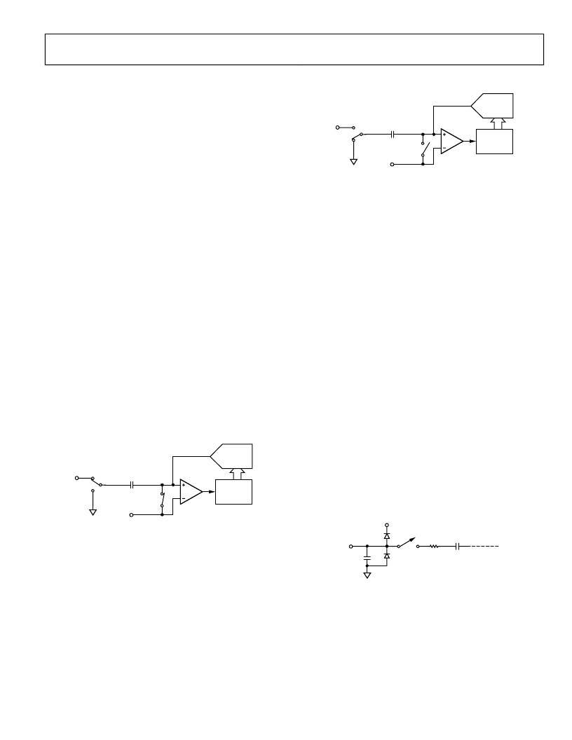
CONVERTER OPERATION
The AD7940 is a 14-bit, successive approximation ADC based
around a capacitive DAC. The AD7940 can convert analog
input signals in the 0 V to V
DD
range. Figure 11 and Figure 12
show simplified schematics of the ADC. The ADC comprises of
control logic, SAR, and a capacitive DAC. Figure 11 shows the
ADC during its acquisition phase. SW2 is closed and SW1 is in
Position A. The comparator is held in a balanced condition and
the sampling capacitor acquires the signal on the selected V
IN
channel.
0
CAPACITIVE
DAC
CONTROL
LOGIC
SAMPLING
CAPACITOR
COMPARATOR
ACQUISITION
PHASE
A
B
SW1
V
DD
/2
SW2
V
IN
Figure 11. ADC Acquisition Phase
When the ADC starts a conversion, SW2 will open and SW1
will move to Position B, causing the comparator to become
unbalanced (Figure 12). The control logic and the capacitive
DAC are used to add and subtract fixed amounts of charge
from the sampling capacitor to bring the comparator back into
a balanced condition. When the comparator is rebalanced, the
conversion is complete. The control logic generates the ADC
output code (see the ADC Transfer Function section).
0
CAPACITIVE
DAC
CONTROL
LOGIC
SAMPLING
CAPACITOR
COMPARATOR
CONVERSION
PHASE
A
B
SW1
V
DD
/2
SW2
V
IN
Figure 12. ADC Conversion Phase
ANALOG INPUT
Figure 13 shows an equivalent circuit of the analog input struc-
ture of the AD7940. The two diodes, D1 and D2, provide ESD
protection for the analog inputs. Care must be taken to ensure
that the analog input signal never exceeds the supply rails by
more than 300 mV. This will cause these diodes to become
forward-biased and to start conducting current into the sub-
strate. The maximum current these diodes can conduct without
causing irreversible damage to the part is 10 mA. Capacitor C1
in Figure 13 is typically about 5 pF and primarily can be attrib-
uted to pin capacitance. Resistor R1 is a lumped component
made up of the on resistance of a switch (track-and-hold
switch). This resistor is typically about 25 . Capacitor C2 is the
ADC sampling capacitor and has a capacitance of 25 pF typi-
cally. For ac applications, removing high frequency components
from the analog input signal is recommended by use of an RC
low-pass filter on the relevant analog input pin. In applications
where harmonic distortion and signal-to-noise ratio are critical,
the analog input should be driven from a low impedance source.
Large source impedances will significantly affect the ac per-
formance of the ADC. This may necessitate the use of an input
buffer amplifier. The choice of the op amp will be a function of
the particular application. When no amplifier is used to drive
the analog input, the source impedance should be limited to low
values. The maximum source impedance will depend on the
amount of total harmonic distortion (THD) that can be toler-
ated. The THD will increase as the source impedance increases,
and performance will degrade (see Figure 8).
0
R1
C2
30pF
CONVERSION PHASE - SWITCH OPEN
TRACK PHASE - SWITCH CLOSED
V
IN
V
DD
C1
4pF
D1
D2
Figure 13. Equivalent Analog Input Circuit
相關(guān)PDF資料 |
PDF描述 |
|---|---|
| AD7683ARMRL7 | 16-Bit, 100 kSPS PulSAR ADC in MSOP/QFN |
| AD7683BRM | 16-Bit, 100 kSPS PulSAR ADC in MSOP/QFN |
| AD7940 | 3mW, 100kSPS, 14-Bit ADC in 6-Lead SOT-23 |
| AD7683BRMRL7 | 16-Bit, 100 kSPS PulSAR ADC in MSOP/QFN |
| AD7943AN-B | +3.3 V/+5 V Multiplying 12-Bit DACs |
相關(guān)代理商/技術(shù)參數(shù) |
參數(shù)描述 |
|---|---|
| AD7683ARMRL7 | 制造商:Analog Devices 功能描述:ADC Single SAR 100ksps 16-bit Serial 8-Pin MSOP T/R |
| AD7683ARMZ | 功能描述:IC ADC 16BIT 100KSPS 8-MSOP RoHS:是 類別:集成電路 (IC) >> 數(shù)據(jù)采集 - 模數(shù)轉(zhuǎn)換器 系列:PulSAR® 標(biāo)準(zhǔn)包裝:1 系列:microPOWER™ 位數(shù):8 采樣率(每秒):1M 數(shù)據(jù)接口:串行,SPI? 轉(zhuǎn)換器數(shù)目:1 功率耗散(最大):- 電壓電源:模擬和數(shù)字 工作溫度:-40°C ~ 125°C 安裝類型:表面貼裝 封裝/外殼:24-VFQFN 裸露焊盤 供應(yīng)商設(shè)備封裝:24-VQFN 裸露焊盤(4x4) 包裝:Digi-Reel® 輸入數(shù)目和類型:8 個(gè)單端,單極 產(chǎn)品目錄頁面:892 (CN2011-ZH PDF) 其它名稱:296-25851-6 |
| AD7683ARMZRL7 | 功能描述:IC ADC 16BIT SAR 100KSPS 8MSOP RoHS:是 類別:集成電路 (IC) >> 數(shù)據(jù)采集 - 模數(shù)轉(zhuǎn)換器 系列:PulSAR® 標(biāo)準(zhǔn)包裝:1,000 系列:- 位數(shù):16 采樣率(每秒):45k 數(shù)據(jù)接口:串行 轉(zhuǎn)換器數(shù)目:2 功率耗散(最大):315mW 電壓電源:模擬和數(shù)字 工作溫度:0°C ~ 70°C 安裝類型:表面貼裝 封裝/外殼:28-SOIC(0.295",7.50mm 寬) 供應(yīng)商設(shè)備封裝:28-SOIC W 包裝:帶卷 (TR) 輸入數(shù)目和類型:2 個(gè)單端,單極 |
| AD7683BCPZRL | 功能描述:IC ADC 16BIT 100KSPS 8LFCSP RoHS:是 類別:集成電路 (IC) >> 數(shù)據(jù)采集 - 模數(shù)轉(zhuǎn)換器 系列:PulSAR® 標(biāo)準(zhǔn)包裝:1,000 系列:- 位數(shù):16 采樣率(每秒):45k 數(shù)據(jù)接口:串行 轉(zhuǎn)換器數(shù)目:2 功率耗散(最大):315mW 電壓電源:模擬和數(shù)字 工作溫度:0°C ~ 70°C 安裝類型:表面貼裝 封裝/外殼:28-SOIC(0.295",7.50mm 寬) 供應(yīng)商設(shè)備封裝:28-SOIC W 包裝:帶卷 (TR) 輸入數(shù)目和類型:2 個(gè)單端,單極 |
| AD7683BCPZRL7 | 功能描述:IC ADC 16BIT 100KSPS 8LFCSP RoHS:是 類別:集成電路 (IC) >> 數(shù)據(jù)采集 - 模數(shù)轉(zhuǎn)換器 系列:PulSAR® 標(biāo)準(zhǔn)包裝:1,000 系列:- 位數(shù):16 采樣率(每秒):45k 數(shù)據(jù)接口:串行 轉(zhuǎn)換器數(shù)目:2 功率耗散(最大):315mW 電壓電源:模擬和數(shù)字 工作溫度:0°C ~ 70°C 安裝類型:表面貼裝 封裝/外殼:28-SOIC(0.295",7.50mm 寬) 供應(yīng)商設(shè)備封裝:28-SOIC W 包裝:帶卷 (TR) 輸入數(shù)目和類型:2 個(gè)單端,單極 |
發(fā)布緊急采購(gòu),3分鐘左右您將得到回復(fù)。