- 您現(xiàn)在的位置:買賣IC網(wǎng) > PDF目錄373927 > AD7683ARM (ANALOG DEVICES INC) 16-Bit, 100 kSPS PulSAR ADC in MSOP/QFN PDF資料下載
參數(shù)資料
| 型號: | AD7683ARM |
| 廠商: | ANALOG DEVICES INC |
| 元件分類: | ADC |
| 英文描述: | 16-Bit, 100 kSPS PulSAR ADC in MSOP/QFN |
| 中文描述: | 1-CH 16-BIT SUCCESSIVE APPROXIMATION ADC, SERIAL ACCESS, PDSO8 |
| 封裝: | MO-187AA, MSOP-8 |
| 文件頁數(shù): | 17/20頁 |
| 文件大小: | 480K |
| 代理商: | AD7683ARM |
AD7940
MICROPROCESSOR INTERFACING
The serial interface on the AD7940 allows the part to be directly
connected to a range of many different microprocessors. This
section explains how to interface the AD7940 with some of the
more common microcontroller and DSP serial interface
protocols.
Rev. 0 | Page 17 of 20
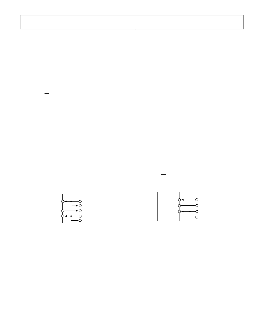
AD7940 TO TMS320C541
The serial interface on the TMS320C541 uses a continuous
serial clock and frame synchronization signals to synchronize
the data transfer operations with peripheral devices such as the
AD7940. The CS input allows easy interfacing between the
TMS320C541 and the AD7940 with no glue logic required. The
serial port of the TMS320C541 is set up to operate in burst
mode with internal CLKX (TX serial clock) and FSX (TX frame
sync). The serial port control register (SPC) must have the
following setup:
FO = 0
FSM = 1
MCM = 1
TXM = 1
The format bit, FO, must be set to 1 to set the word length to
8 bits, in order to implement the power-down mode on the
AD7940. The connection diagram is shown in Figure 21. It
should be noted that for signal processing applications, it is
imperative that the frame synchronization signal from the
TMS320C541 provide equidistant sampling.
0
AD7940*
TMS320C541*
*ADDITIONAL PINS OMITTED FOR CLARITY
SDATA
DR
CS
FSX
FSR
SCLK
CLKX
CLKR
Figure 21. Interfacing to the TMS320C541
AD7940 TO ADSP-218x
The ADSP-218x family of DSPs can be interfaced directly to the
AD7940 with no glue logic required. The SPORT control regis-
ter should be set up as follows:
TFSW = RFSW = 1, Alternate Framing
INVRFS = INVTFS = 1, Active Low Frame Signal
DTYPE = 00, Right Justify Data
SLEN = 1111, 16-Bit Data-Words
ISCLK = 1, Internal Serial Clock
TFSR = RFSR = 0, Frame First Word
IRFS = 0
ITFS = 1
To implement power-down mode, SLEN should be set to 0111
to issue an 8-bit SCLK burst.
The connection diagram is shown in Figure 22. The ADSP-218x
has the TFS and RFS of the SPORT tied together, with TFS set
as an output and RFS set as an input. The DSP operates in alter-
nate framing mode, and the SPORT control register is set up as
described. The frame synchronization signal generated on the
TFS is tied to CS, and, as with all signal processing applications,
equidistant sampling is necessary. In this example, the timer
interrupt is used to control the sampling rate of the ADC.
0
SCLK
AD7940*
SDATA
CS
ADSP-218x*
SCLK
*ADDITIONAL PINS OMITTED FOR CLARITY
DR
RFS
TFS
Figure 22. Interfacing to the ADSP-218x
The timer register is loaded with a value that provides an
interrupt at the required sample interval. When an interrupt is
received, the values in the transmit autobuffer start to be trans-
mitted and TFS is generated. The TFS is used to control the
RFS and, therefore, the reading of data. The data is stored in the
receive autobuffer for processing or to be shifted later. The fre-
quency of the serial clock is set in the SCLKDIV register. When
the instruction to transmit with TFS is given, i.e., TX0 = AX0,
the state of the SCLK is checked. The DSP waits until the SCLK
has gone high, low, and high before transmission will start. If
the timer and SCLK values are chosen such that the instruction
to transmit occurs on or near the rising edge of SCLK, the data
may be transmitted, or it may wait until the next clock edge.
相關PDF資料 |
PDF描述 |
|---|---|
| AD7683ARMRL7 | 16-Bit, 100 kSPS PulSAR ADC in MSOP/QFN |
| AD7683BRM | 16-Bit, 100 kSPS PulSAR ADC in MSOP/QFN |
| AD7940 | 3mW, 100kSPS, 14-Bit ADC in 6-Lead SOT-23 |
| AD7683BRMRL7 | 16-Bit, 100 kSPS PulSAR ADC in MSOP/QFN |
| AD7943AN-B | +3.3 V/+5 V Multiplying 12-Bit DACs |
相關代理商/技術參數(shù) |
參數(shù)描述 |
|---|---|
| AD7683ARMRL7 | 制造商:Analog Devices 功能描述:ADC Single SAR 100ksps 16-bit Serial 8-Pin MSOP T/R |
| AD7683ARMZ | 功能描述:IC ADC 16BIT 100KSPS 8-MSOP RoHS:是 類別:集成電路 (IC) >> 數(shù)據(jù)采集 - 模數(shù)轉(zhuǎn)換器 系列:PulSAR® 標準包裝:1 系列:microPOWER™ 位數(shù):8 采樣率(每秒):1M 數(shù)據(jù)接口:串行,SPI? 轉(zhuǎn)換器數(shù)目:1 功率耗散(最大):- 電壓電源:模擬和數(shù)字 工作溫度:-40°C ~ 125°C 安裝類型:表面貼裝 封裝/外殼:24-VFQFN 裸露焊盤 供應商設備封裝:24-VQFN 裸露焊盤(4x4) 包裝:Digi-Reel® 輸入數(shù)目和類型:8 個單端,單極 產(chǎn)品目錄頁面:892 (CN2011-ZH PDF) 其它名稱:296-25851-6 |
| AD7683ARMZRL7 | 功能描述:IC ADC 16BIT SAR 100KSPS 8MSOP RoHS:是 類別:集成電路 (IC) >> 數(shù)據(jù)采集 - 模數(shù)轉(zhuǎn)換器 系列:PulSAR® 標準包裝:1,000 系列:- 位數(shù):16 采樣率(每秒):45k 數(shù)據(jù)接口:串行 轉(zhuǎn)換器數(shù)目:2 功率耗散(最大):315mW 電壓電源:模擬和數(shù)字 工作溫度:0°C ~ 70°C 安裝類型:表面貼裝 封裝/外殼:28-SOIC(0.295",7.50mm 寬) 供應商設備封裝:28-SOIC W 包裝:帶卷 (TR) 輸入數(shù)目和類型:2 個單端,單極 |
| AD7683BCPZRL | 功能描述:IC ADC 16BIT 100KSPS 8LFCSP RoHS:是 類別:集成電路 (IC) >> 數(shù)據(jù)采集 - 模數(shù)轉(zhuǎn)換器 系列:PulSAR® 標準包裝:1,000 系列:- 位數(shù):16 采樣率(每秒):45k 數(shù)據(jù)接口:串行 轉(zhuǎn)換器數(shù)目:2 功率耗散(最大):315mW 電壓電源:模擬和數(shù)字 工作溫度:0°C ~ 70°C 安裝類型:表面貼裝 封裝/外殼:28-SOIC(0.295",7.50mm 寬) 供應商設備封裝:28-SOIC W 包裝:帶卷 (TR) 輸入數(shù)目和類型:2 個單端,單極 |
| AD7683BCPZRL7 | 功能描述:IC ADC 16BIT 100KSPS 8LFCSP RoHS:是 類別:集成電路 (IC) >> 數(shù)據(jù)采集 - 模數(shù)轉(zhuǎn)換器 系列:PulSAR® 標準包裝:1,000 系列:- 位數(shù):16 采樣率(每秒):45k 數(shù)據(jù)接口:串行 轉(zhuǎn)換器數(shù)目:2 功率耗散(最大):315mW 電壓電源:模擬和數(shù)字 工作溫度:0°C ~ 70°C 安裝類型:表面貼裝 封裝/外殼:28-SOIC(0.295",7.50mm 寬) 供應商設備封裝:28-SOIC W 包裝:帶卷 (TR) 輸入數(shù)目和類型:2 個單端,單極 |
發(fā)布緊急采購,3分鐘左右您將得到回復。