- 您現在的位置:買賣IC網 > PDF目錄373927 > AD7685 (Analog Devices, Inc.) 3mW, 100kSPS, 14-Bit ADC in 6-Lead SOT-23 PDF資料下載
參數資料
| 型號: | AD7685 |
| 廠商: | Analog Devices, Inc. |
| 元件分類: | ADC |
| 英文描述: | 3mW, 100kSPS, 14-Bit ADC in 6-Lead SOT-23 |
| 中文描述: | 3MW的,100ksps的14位ADC的6引腳SOT - 23 |
| 文件頁數: | 16/20頁 |
| 文件大小: | 480K |
| 代理商: | AD7685 |
AD7940
SERIAL INTERFACE
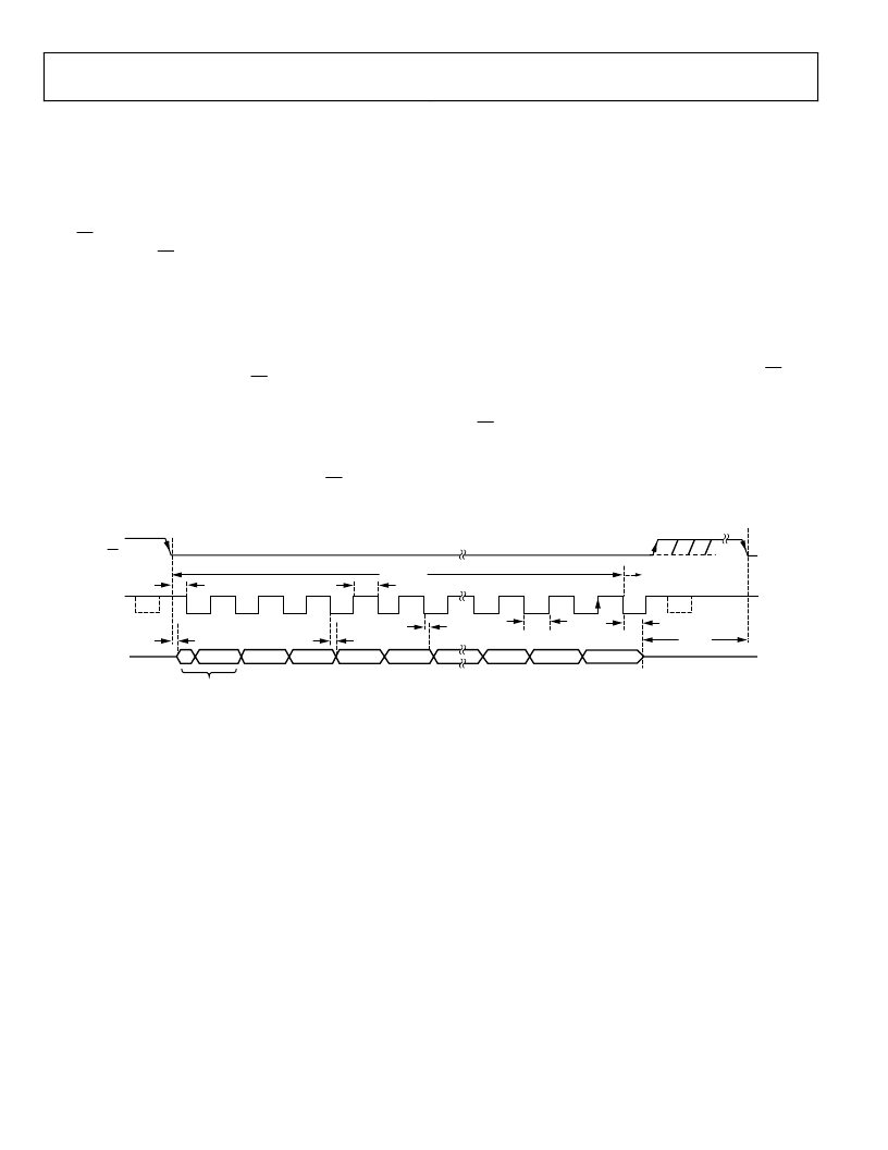
Figure 20 shows the detailed timing diagram for serial interfac-
ing to the AD7940. The serial clock provides the conversion
clock and also controls the transfer of information from the
AD7940 during conversion.
Rev. 0 | Page 16 of 20
The CS signal initiates the data transfer and conversion process.
The falling edge of CS puts the track-and-hold into hold mode,
takes the bus out of three-state, and samples the analog input.
The conversion is also initiated at this point and will require at
least 16 SCLK cycles to complete. Once 15 SCLK falling edges
have elapsed, the track-and-hold will go back into track mode
on the next SCLK rising edge as shown in Figure 20 at Point B.
On the 16th SCLK falling edge, the SDATA line will go back
into three-state. If the rising edge of CS occurs before 16 SCLKs
have elapsed, the conversion will be terminated and the SDATA
line will go back into three-state; otherwise SDATA returns to
three-state on the 16th SCLK falling edge as shown in Figure 20.
Sixteen serial clock cycles are required to perform the conver-
sion process and to access data from the AD7940. CS going low
provides the first leading zero to be read in by the microcontroller
or DSP. The remaining data is then clocked out by subsequent
SCLK falling edges beginning with the second leading zero, thus
the first falling clock edge on the serial clock has the first leading
zero provided and also clocks out the second leading zero. The
data transfer will consist of two leading zeros followed by the 14
bits of data. The final bit in the data transfer is valid on the 16th
falling edge, having been clocked out on the previous (15th)
falling edge.
It is also possible to take valid data on each SCLK rising edge
rather than falling edge, since the SCLK cycle time is long
enough to ensure the data is ready on the rising edge of SCLK.
However, the first leading zero will still be driven by the CS
falling edge, and so it can be taken only on the first SCLK falling
edge. It may be ignored, and the first rising edge of SCLK after
the CS falling edge would have the second leading zero pro-
vided and the 15th rising SCLK edge would have DB0 provided.
This method may not work with most microcontrollers/DSPs, but
could possibly be used with FPGAs and ASICs.
0
t
4
t
CONVERT
2 LEADING ZEROS
3-STATE
3-STATE
B
SCLK
1
2
3
4
5
13
14
15
16
SDATA
0
ZERO
DB13
DB12
DB11
DB10
DB2
DB1
DB0
CS
t
2
t
3
t
6
t
7
t
5
t
8
t
QUIET
Figure 20. AD7940 Serial Interface Timing Diagram
相關PDF資料 |
PDF描述 |
|---|---|
| AD7687 | +3.3V, 2.7Gbps Dual 2 x 2 Crosspoint Switch |
| AD7683ARM | 16-Bit, 100 kSPS PulSAR ADC in MSOP/QFN |
| AD7683ARMRL7 | 16-Bit, 100 kSPS PulSAR ADC in MSOP/QFN |
| AD7683BRM | 16-Bit, 100 kSPS PulSAR ADC in MSOP/QFN |
| AD7940 | 3mW, 100kSPS, 14-Bit ADC in 6-Lead SOT-23 |
相關代理商/技術參數 |
參數描述 |
|---|---|
| AD76851 | 制造商:AD 制造商全稱:Analog Devices 功能描述:14-Bit, 500 kSPS PulSAR ADC in MSOP |
| AD7685ACPZRL | 功能描述:IC ADC 16BIT SAR 250KSPS 10LFCSP RoHS:是 類別:集成電路 (IC) >> 數據采集 - 模數轉換器 系列:PulSAR® 標準包裝:1,000 系列:- 位數:16 采樣率(每秒):45k 數據接口:串行 轉換器數目:2 功率耗散(最大):315mW 電壓電源:模擬和數字 工作溫度:0°C ~ 70°C 安裝類型:表面貼裝 封裝/外殼:28-SOIC(0.295",7.50mm 寬) 供應商設備封裝:28-SOIC W 包裝:帶卷 (TR) 輸入數目和類型:2 個單端,單極 |
| AD7685ACPZRL7 | 功能描述:IC ADC 16BIT SAR 250KSPS 10LFCSP RoHS:是 類別:集成電路 (IC) >> 數據采集 - 模數轉換器 系列:PulSAR® 標準包裝:1,000 系列:- 位數:16 采樣率(每秒):45k 數據接口:串行 轉換器數目:2 功率耗散(最大):315mW 電壓電源:模擬和數字 工作溫度:0°C ~ 70°C 安裝類型:表面貼裝 封裝/外殼:28-SOIC(0.295",7.50mm 寬) 供應商設備封裝:28-SOIC W 包裝:帶卷 (TR) 輸入數目和類型:2 個單端,單極 |
| AD7685ARM | 制造商:Analog Devices 功能描述:ADC Single SAR 250ksps 16-bit Serial 10-Pin MSOP 制造商:Rochester Electronics LLC 功能描述:16-BIT 100KSPS I.C. - Bulk |
| AD7685ARMRL7 | 制造商:Analog Devices 功能描述:ADC Single SAR 250ksps 16-bit Serial 10-Pin MSOP T/R |
發布緊急采購,3分鐘左右您將得到回復。