- 您現在的位置:買賣IC網 > PDF目錄373913 > AD7701 (Analog Devices, Inc.) LC2MOS 16-Bit A/D Converter PDF資料下載
參數資料
| 型號: | AD7701 |
| 廠商: | Analog Devices, Inc. |
| 英文描述: | LC2MOS 16-Bit A/D Converter |
| 中文描述: | LC2MOS 16位A / D轉換器 |
| 文件頁數: | 8/16頁 |
| 文件大小: | 312K |
| 代理商: | AD7701 |
AD7701
REV. D
–8–
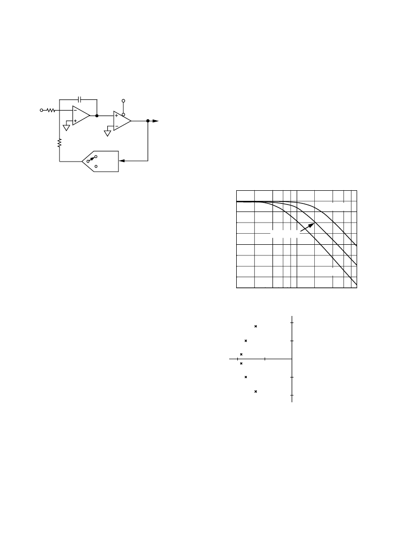
FILT E R CHARACT E RIST ICS
T he cutoff frequency of the digital filter is f
CLK
/409600. At the
maximum clock frequency of 4.096 MHz, the cutoff frequency
of the filter is 10 Hz and the output rate is 4 kHz.
Figure 10 shows the filter frequency response. T his is a 6-pole
Gaussian response that provides 55 dB of 60 Hz rejection for a
10 Hz cutoff frequency. If the clock frequency is halved to give a
5 Hz cutoff, 60 Hz rejection is better than 90 dB. A normalized
s-domain pole-zero plot of the filter is shown in Figure 11.
T he response of the filter is defined by:
H(x) =
[1
+
0.693
x
2
+
0.240
x
4
+
0.0555
x
6
+
0.00962
x
8
+
0.00133
x
10
+
0.000154
x
12
]
–0.5
where:
x
= f/f
3 dB
, f
3 dB
= f
CLK IN
/409600,
and
f
is the frequency of interest.
f
CLK
= 2MHz
f
CLK
= 1MHz
f
CLK
= 4MHz
1
10
100
FREQUENCY – Hz
20
0
–20
–40
–60
–80
–100
–120
–140
–160
G
Figure 10. Frequency Response of AD7701 Filter
jw
s
0
j1
j2
–2
–1
–j1
–j2
S1,2 = –1.4663 + j1.8191
S3,4 = –1.7553 + j1.0005
S5,6 = –1.8739 + j0.32272
Figure 11. Normalized Pole-Zero Plot of AD7701 Filter
Since the AD7701 contains this on-chip, low-pass filtering,
there is a settling time associated with step function inputs, and
data will be invalid after a step change until the settling time has
elapsed. T he AD7701 is therefore unsuitable for high speed
multiplexing, where channels are switched and converted se-
quentially at high rates, as switching between channels can
cause a step change in the input. Rather, it is intended for dis-
tributed converter systems using one ADC per channel.
However, slow multiplexing of the AD7701 is possible, provided
that the settling time is allowed to elapse before data for the new
channel is accessed.
Sigma-delta ADCs are generally described by the order of the
analog low-pass filter. A simple example of a first order sigma-
delta ADC is shown in Figure 9. T his contains only a first-order
low-pass filter or integrator. It also illustrates the derivation of
the alternative name for these devices: Charge-Balancing ADCs.
C
R
R
A
IN
INTEGRATOR
TO DIGITAL
FILTER
CLOCK
1-BIT DAC
STROBED
COMPARATOR
+V
REF
–V
REF
Figure 9. SEC Basic Charge-Balancing ADC
T he term charge-balancing comes from the fact that this system
is a negative feedback loop that tries to keep the net charge on
the integrator capacitor at zero, by balancing charge injected by
the input voltage with charge injected by the 1-bit DAC. When
the analog input is zero, the only contribution to the integrator
output comes from the 1-bit DAC. For the net charge on the
integrator capacitor to be zero, the DAC output must spend half
its time at +1 V and half its time at –1 V. Assuming ideal
components, the duty cycle of the comparator will be 50%.
When a positive analog input is applied, the output of the 1-bit
DAC must spend a larger proportion of the time at +1 V, so the
duty cycle of the comparator increases. When a negative input
voltage is applied, the duty cycle decreases.
T he AD7701 uses a second-order sigma-delta modulator and a
sophisticated digital filter that provides a rolling average of the
sampled output. After power-up or if there is a step change in
the input voltage, there is a settling time that must elapse before
valid data is obtained.
DIGIT AL FILT E RING
T he AD7701’s digital filter behaves like a similar analog filter,
with a few minor differences.
First, since digital filtering occurs after the A to D conversion
process, it can remove noise injected during the conversion
process. Analog filtering cannot do this.
On the other hand, analog filtering can remove noise super-
imposed on the analog signal before it reaches the ADC. Digital
filtering cannot do this and noise peaks riding on signals near
full scale have the potential to saturate the analog modulator
and digital filter, even though the average value of the signal is
within limits. T o alleviate this problem, the AD7701 has over-
range headroom built into the sigma-delta modulator and digital
filter which allows overrange excursions of 100 mV. If noise
signals are larger than this, consideration should be given to
analog input filtering, or to reducing the gain in the input
channel so that a full-scale input (2.5 V) gives only a half-scale
input to the AD7701 (1.25 V). T his will provide an overrange
capability greater than 100% at the expense of reducing the
dynamic range by 1 bit (50%).
相關PDF資料 |
PDF描述 |
|---|---|
| AD7703 | LC2MOS 20-Bit A/D Converter |
| AD7703AN | LC2MOS 20-Bit A/D Converter |
| AD7703AQ | LC2MOS 20-Bit A/D Converter |
| AD7703AR | LC2MOS 20-Bit A/D Converter |
| AD7703BN | LC2MOS 20-Bit A/D Converter |
相關代理商/技術參數 |
參數描述 |
|---|---|
| AD7701AN | 功能描述:IC ADC 16BIT LC2MOS 20-DIP RoHS:否 類別:集成電路 (IC) >> 數據采集 - 模數轉換器 系列:- 標準包裝:1 系列:- 位數:14 采樣率(每秒):83k 數據接口:串行,并聯 轉換器數目:1 功率耗散(最大):95mW 電壓電源:雙 ± 工作溫度:0°C ~ 70°C 安裝類型:通孔 封裝/外殼:28-DIP(0.600",15.24mm) 供應商設備封裝:28-PDIP 包裝:管件 輸入數目和類型:1 個單端,雙極 |
| AD7701ANZ | 功能描述:IC ADC 16BIT LC2MOS 20-DIP RoHS:是 類別:集成電路 (IC) >> 數據采集 - 模數轉換器 系列:- 標準包裝:1 系列:microPOWER™ 位數:8 采樣率(每秒):1M 數據接口:串行,SPI? 轉換器數目:1 功率耗散(最大):- 電壓電源:模擬和數字 工作溫度:-40°C ~ 125°C 安裝類型:表面貼裝 封裝/外殼:24-VFQFN 裸露焊盤 供應商設備封裝:24-VQFN 裸露焊盤(4x4) 包裝:Digi-Reel® 輸入數目和類型:8 個單端,單極 產品目錄頁面:892 (CN2011-ZH PDF) 其它名稱:296-25851-6 |
| AD7701AQ | 制造商:AD 制造商全稱:Analog Devices 功能描述:LC2MOS 16-Bit A/D Converter |
| AD7701AR | 功能描述:IC ADC 16BIT LC2MOS 20-SOIC RoHS:否 類別:集成電路 (IC) >> 數據采集 - 模數轉換器 系列:- 標準包裝:1 系列:- 位數:14 采樣率(每秒):83k 數據接口:串行,并聯 轉換器數目:1 功率耗散(最大):95mW 電壓電源:雙 ± 工作溫度:0°C ~ 70°C 安裝類型:通孔 封裝/外殼:28-DIP(0.600",15.24mm) 供應商設備封裝:28-PDIP 包裝:管件 輸入數目和類型:1 個單端,雙極 |
| AD7701AR-REEL | 制造商:Rochester Electronics LLC 功能描述:- Tape and Reel |
發布緊急采購,3分鐘左右您將得到回復。