- 您現在的位置:買賣IC網 > PDF目錄373913 > AD7701SQ (ANALOG DEVICES INC) LC2MOS 16-Bit A/D Converter PDF資料下載
參數資料
| 型號: | AD7701SQ |
| 廠商: | ANALOG DEVICES INC |
| 元件分類: | ADC |
| 英文描述: | LC2MOS 16-Bit A/D Converter |
| 中文描述: | 1-CH 16-BIT DELTA-SIGMA ADC, SERIAL ACCESS, CDIP20 |
| 封裝: | CERDIP-20 |
| 文件頁數: | 13/16頁 |
| 文件大小: | 312K |
| 代理商: | AD7701SQ |
–13–
REV. D
AD7701
AGND
AD7701
DGND
AV
DD
V
REF
10k
10k
0.1
μ
F
0.1
μ
F
DV
DD
AV
SS
DV
SS
0.1
μ
F
REF
10V
±
1V
AD707
0.1
μ
F
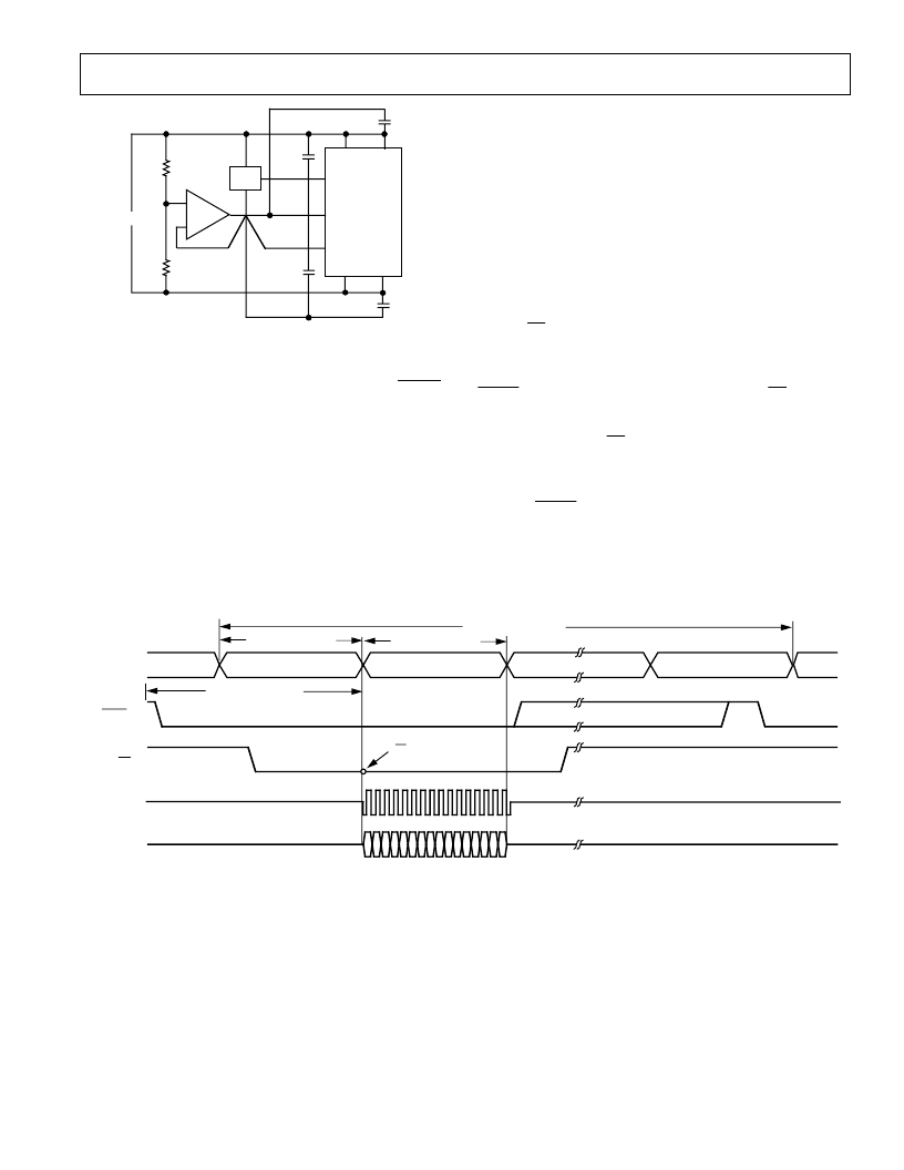
Figure 17. Single Supply Operation
SLE E P MODE
T he low power standby mode is initiated by taking the
SLEEP
input low, which shuts down all analog and digital circuits and
reduces power consumption to 10
μ
W. T he calibration coeffi-
cients are still retained in memory, but as the converter has been
quiescent, it is necessary to wait for the filter settling time
(507,904 cycles) before accessing the output data.
DIGIT AL INT E RFACE
T he AD7701’s serial communications port allows easy inter-
facing to industry-standard microprocessors. T hree different
modes of operations are available, optimized for different types
of interface.
SY NCHRONOUS SE LF-CLOCK ING MODE (SSC)
T he SSC mode (MODE pin high) allows easy interfacing to
serial-parallel conversion circuits in systems with parallel data
communication. T his mode allows interfacing to 74X X 299
Universal Shift registers without any additional decoding. T he
SSC mode can also be used with microprocessors such as the
68HC11 and 68HC05, which allow an external device to clock
their serial port.
Figure 18 shows the timing diagram for the SSC mode. Data is
clocked out by an internally generated serial clock. T he AD7701
divides each sampling interval into sixteen distinct periods.
Eight periods of 64 clock pulses are for analog settling and eight
periods of 64 clock pulses are for digital computation. T he
status of
CS
is polled at the beginning of each digital computation
period. If it is low at any of these times then SCLK will become
active and the data word currently in the output register will be
transmitted, MSB first. After the LSB has been transmitted
DRDY
goes high and SDAT A goes three-state. If
CS
, having
been brought low, is taken high again at any time during data
transmission, SDAT A and SCLK will go three-state after the
current bit finishes. If
CS
is subsequently brought low,
transmission will resume with the next bit during the sub-
sequent digital computation period. If transmission has not been
initiated and completed by the time the next data word is
available,
DRDY
will go high for four clock cycles then low
again as the new word is loaded into the output register.
A more detailed diagram of the data transmission in the SSC
mode is shown in Figure 19. Data bits change on the falling
edge of SCLK and are valid on the rising edge of SCLK .
ANALOG SETTLING
DIGITAL COMPUTATION
SCLK (O)
SDATA (O)
HI-Z
HI-Z
HI-Z
HI-Z
MSB
LSB
DRDY (O)
DIGITAL COMPUTATION
CS POLLED
CS (I)
INTERNAL
STATUS
72 CLKIN CYCLES
64 CLKIN CYCLES
64 CLKIN CYCLES
1024 CLKIN CYCLES
Figure 18. Timing Diagram for SSC Data Transmission Mode
相關PDF資料 |
PDF描述 |
|---|---|
| AD7701TQ | LC2MOS 16-Bit A/D Converter |
| AD7701 | LC2MOS 16-Bit A/D Converter |
| AD7703 | LC2MOS 20-Bit A/D Converter |
| AD7703AN | LC2MOS 20-Bit A/D Converter |
| AD7703AQ | LC2MOS 20-Bit A/D Converter |
相關代理商/技術參數 |
參數描述 |
|---|---|
| AD7701TQ | 制造商:AD 制造商全稱:Analog Devices 功能描述:LC2MOS 16-Bit A/D Converter |
| AD7703 | 制造商:AD 制造商全稱:Analog Devices 功能描述:LC2MOS 20-Bit A/D Converter |
| AD7703AN | 功能描述:IC ADC 20BIT LC2MOS 20-DIP RoHS:否 類別:集成電路 (IC) >> 數據采集 - 模數轉換器 系列:- 標準包裝:1 系列:- 位數:14 采樣率(每秒):83k 數據接口:串行,并聯 轉換器數目:1 功率耗散(最大):95mW 電壓電源:雙 ± 工作溫度:0°C ~ 70°C 安裝類型:通孔 封裝/外殼:28-DIP(0.600",15.24mm) 供應商設備封裝:28-PDIP 包裝:管件 輸入數目和類型:1 個單端,雙極 |
| AD7703ANZ | 功能描述:IC ADC 20BIT LC2MOS MONO 20DIP RoHS:是 類別:集成電路 (IC) >> 數據采集 - 模數轉換器 系列:- 其它有關文件:TSA1204 View All Specifications 標準包裝:1 系列:- 位數:12 采樣率(每秒):20M 數據接口:并聯 轉換器數目:2 功率耗散(最大):155mW 電壓電源:模擬和數字 工作溫度:-40°C ~ 85°C 安裝類型:表面貼裝 封裝/外殼:48-TQFP 供應商設備封裝:48-TQFP(7x7) 包裝:Digi-Reel® 輸入數目和類型:4 個單端,單極;2 個差分,單極 產品目錄頁面:1156 (CN2011-ZH PDF) 其它名稱:497-5435-6 |
| AD7703AQ | 制造商:Rochester Electronics LLC 功能描述:- Bulk |
發布緊急采購,3分鐘左右您將得到回復。