- 您現在的位置:買賣IC網 > PDF目錄373913 > AD7703 (Analog Devices, Inc.) LC2MOS 20-Bit A/D Converter PDF資料下載
參數資料
| 型號: | AD7703 |
| 廠商: | Analog Devices, Inc. |
| 英文描述: | LC2MOS 20-Bit A/D Converter |
| 中文描述: | LC2MOS 20位A / D轉換器 |
| 文件頁數: | 11/16頁 |
| 文件大小: | 251K |
| 代理商: | AD7703 |
AD7703
REV. D
–11–
T able V. AD7703 Output Coding
I
NPUT VOLT AGE , UNIPOLAR MODE INPUT VOLT AGE , BIPOLAR MODE
System Cal
Self Cal
Output Codes
Self-Cal
System Cal
>(
S
GAIN
–1.5 LSB)
>
(V
REF
– 1.5 LSB)
FFFFF
>
(V
REF
–1.5 LSB)
>
(S
GAIN
– 1.5 LSB)
S
GAIN
– 1.5 LSB
V
REF
– 1.5 LSB
FFFFF
FFFFE
V
REF
– 1.5 LSB
S
GAIN
– 1.5 LSB
(S
GAIN
– S
OFF
)/2 – 0.5 LSB
(V
REF
– V
AGND
)/2 – 0.5 LSB
80000
7FFFF
V
AGND
– 0.5 LSB
S
OFF
– 0.5 LSB
S
OFF
+ 0.5 LSB
V
AGND
+ 0.5 LSB
00001
00000
–V
REF
+ 0.5 LSB
–S
GAIN
+ 2 S
OFF
+ 0.5 LSB
<
(S
OFF
+ 0.5 LSB)
<
(V
AGND
+ 0.5 LSB)
00000
<
(–V
REF
+ 0.5 LSB)
<(–S
GAIN
+2 S
OFF
+ 0.5 LSB)
updated at a rate determined by the master clock, therefore the
amount of offset drift which occurs will be proportional to the
elapsed time between samples. T hus, to minimize offset drift at
higher temperatures, higher CLK IN rates are recommended.
Gain drift within the converter depends mainly upon the tem-
perature tracking of the internal capacitors. It is not affected by
leakage currents so that it is significantly less than offset drift.
T he typical gain drift of the AD7703 is less than 40 LSBs over
the specified temperature range.
Measurement errors due to offset drift or gain drift can be elimi-
nated at any time by recalibrating the converter. Using the sys-
tem calibration mode can also minimize offset and gain errors in
the signal conditioning circuitry. Integral and differential linear-
ity are not significantly affected by temperature changes.
B
160
0
–80
–160
–240
–320
–55
5
25
105
125
TEMPERATURE –
°
C
80
–35
–15
45
65
85
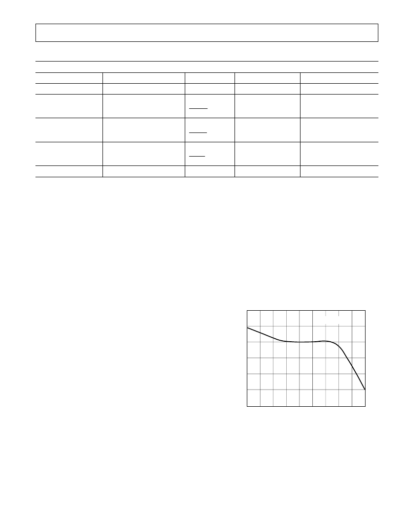
CLKIN = 4.096MHz
Figure 13. Typical Bipolar Offset vs. Temperature after
Calibration at +25
°
C
In the bipolar mode the system offset calibration range is
restricted to
±
0.4 V
REF
. It should be noted that the span
restrictions limit the amount of offset which can be calibrated.
T he span range of the converter in bipolar mode is equidistant
around the voltage used for the zero scale point. When the zero-
scale point is calibrated it must not cause either of the two
endpoints of the bipolar transfer function to exceed the positive
or the negative input overrange points (+V
REF
+ 0.1) V or
–V
REF
+ 0.1) V. If the span range is set to a minimum (0.8 V
REF
)
the offset voltage can move +0.4 V
REF
without causing the end
points of the transfer function to exceed the overrange points.
Alternatively, if the span range is set to 2 V
REF
, the input offset
cannot move more than +0.1 V or –0.1 V before an endpoint of
the transfer function exceeds the input overrange limit.
POWE R-UP AND CALIBRAT ION
A calibration cycle must be carried out after power-up to
initialize the device to a consistent starting condition and correct
calibration. T he CAL pin must be held high for at least four
clock cycles, after which calibration is initiated on the falling
edge of CAL and takes a maximum of 3,145,655 clock cycles
(approximately 768 ms with a 4.096 MHz clock). See T able III.
T he type of calibration cycle initiated by CAL is determined by
the SC1 and SC2 inputs, in accordance with T able III.
Drift Considerations
T he AD7703 uses chopper stabilization techniques to minimize
input offset drift. Charge injection in the analog switches and
leakage currents at the sampling node are the primary sources of
offset voltage drift in the converter. Figure 13 indicates the typi-
cal offset due to temperature changes after calibration at 25
°
C.
Drift is relatively flat up to 75
°
C. Above this temperature, leak-
age current becomes the main source of offset drift. Since leak-
age current doubles approximately every 10
°
C, the offset drifts
accordingly. T he value of the voltage on the sample capacitor is
相關PDF資料 |
PDF描述 |
|---|---|
| AD7703AN | LC2MOS 20-Bit A/D Converter |
| AD7703AQ | LC2MOS 20-Bit A/D Converter |
| AD7703AR | LC2MOS 20-Bit A/D Converter |
| AD7703BN | LC2MOS 20-Bit A/D Converter |
| AD7703BQ | LC2MOS 20-Bit A/D Converter |
相關代理商/技術參數 |
參數描述 |
|---|---|
| AD7703AN | 功能描述:IC ADC 20BIT LC2MOS 20-DIP RoHS:否 類別:集成電路 (IC) >> 數據采集 - 模數轉換器 系列:- 標準包裝:1 系列:- 位數:14 采樣率(每秒):83k 數據接口:串行,并聯 轉換器數目:1 功率耗散(最大):95mW 電壓電源:雙 ± 工作溫度:0°C ~ 70°C 安裝類型:通孔 封裝/外殼:28-DIP(0.600",15.24mm) 供應商設備封裝:28-PDIP 包裝:管件 輸入數目和類型:1 個單端,雙極 |
| AD7703ANZ | 功能描述:IC ADC 20BIT LC2MOS MONO 20DIP RoHS:是 類別:集成電路 (IC) >> 數據采集 - 模數轉換器 系列:- 其它有關文件:TSA1204 View All Specifications 標準包裝:1 系列:- 位數:12 采樣率(每秒):20M 數據接口:并聯 轉換器數目:2 功率耗散(最大):155mW 電壓電源:模擬和數字 工作溫度:-40°C ~ 85°C 安裝類型:表面貼裝 封裝/外殼:48-TQFP 供應商設備封裝:48-TQFP(7x7) 包裝:Digi-Reel® 輸入數目和類型:4 個單端,單極;2 個差分,單極 產品目錄頁面:1156 (CN2011-ZH PDF) 其它名稱:497-5435-6 |
| AD7703AQ | 制造商:Rochester Electronics LLC 功能描述:- Bulk |
| AD7703AR | 功能描述:IC ADC 20BIT LC2MOS 20-SOIC RoHS:否 類別:集成電路 (IC) >> 數據采集 - 模數轉換器 系列:- 標準包裝:1 系列:- 位數:14 采樣率(每秒):83k 數據接口:串行,并聯 轉換器數目:1 功率耗散(最大):95mW 電壓電源:雙 ± 工作溫度:0°C ~ 70°C 安裝類型:通孔 封裝/外殼:28-DIP(0.600",15.24mm) 供應商設備封裝:28-PDIP 包裝:管件 輸入數目和類型:1 個單端,雙極 |
| AD7703AR-REEL | 功能描述:IC ADC 20BIT LC2MOS MONO 20-SOIC RoHS:否 類別:集成電路 (IC) >> 數據采集 - 模數轉換器 系列:- 標準包裝:1 系列:- 位數:14 采樣率(每秒):83k 數據接口:串行,并聯 轉換器數目:1 功率耗散(最大):95mW 電壓電源:雙 ± 工作溫度:0°C ~ 70°C 安裝類型:通孔 封裝/外殼:28-DIP(0.600",15.24mm) 供應商設備封裝:28-PDIP 包裝:管件 輸入數目和類型:1 個單端,雙極 |
發布緊急采購,3分鐘左右您將得到回復。