- 您現(xiàn)在的位置:買賣IC網(wǎng) > PDF目錄373913 > AD7703 (Analog Devices, Inc.) LC2MOS 20-Bit A/D Converter PDF資料下載
參數(shù)資料
| 型號: | AD7703 |
| 廠商: | Analog Devices, Inc. |
| 英文描述: | LC2MOS 20-Bit A/D Converter |
| 中文描述: | LC2MOS 20位A / D轉(zhuǎn)換器 |
| 文件頁數(shù): | 12/16頁 |
| 文件大小: | 251K |
| 代理商: | AD7703 |
AD7703
–12–
REV. D
INPUT SIGNAL CONDIT IONING
Reference voltages from +1 V to +3 V may be used with the
AD7703, with little degradation in performance. Input ranges
that cannot be accommodated by this range of reference voltages
may be achieved by input signal conditioning. T his may take the
form of gain to accommodate a smaller signal range, or passive
attenuation to reduce a larger input voltage range.
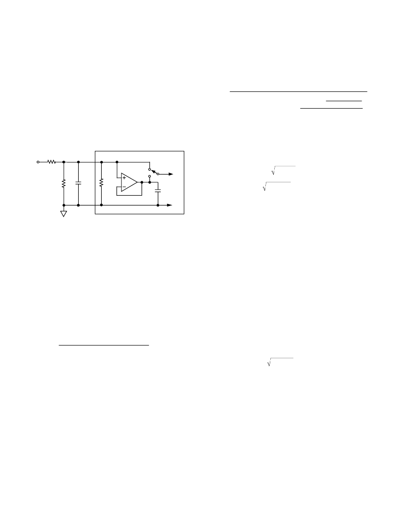
Source Resistance
If passive attenuators are used in front of the AD7703, care
must be taken to ensure that the source impedance is suffi-
ciently low. T he dc input resistance for the AD7703 is over
1 G
. In parallel with this there as a small dynamic load which
varies with the clock frequency (see Figure 14). Each time the
A
IN
R1
R2
C
EXT
AGND
AD7703
V
OS
≤
100mV
C
10pF
V
IN
1G
Figure 14. Equivalent Input Circuit and Input Attenuator
analog input is sampled, a 10 pF capacitor draws a charge
packet of maximum 1 pC (10 pF
3
100 mV) from the analog
source with a frequency f
CLK IN
/256. For a 4.096 MHz CLK IN,
this yields an average current draw of 16 nA. After each sample
the AD7703 allows 62 clock periods for the input voltage to
settle. T he equation which defines settling time is:
V
O
=
V
IN
[1±
e
±
t
/
RC
]
where
V
O
, is the final settled value,
V
IN
, is the value of the input
signal,
R
is the value of the input source resistance,
C
is the
10 pF sample capacitor. T he value of
t
is
equal to 62/f
CLK IN
.
T he following equation can be developed which gives the max-
imum allowable source resistance, R
S(MAX )
for an error of V
E
.
R
S
(
MAX
)
=
62
f
CLKIN
·(10
pF
)·
ln
(100
mV
/
V
E
)
Provided the source resistance is less than this value, the analog
input will settle within the desired error band in the requisite 62
clock periods. Insufficient settling leads to offset errors. T hese
can be calibrated in system calibration schemes.
If a limit of 600 nV (0.25 LSB at 20 bits) is set for the maxi-
mum offset voltage, then the maximum allowable source resis-
tance is 125 k
from the above equation, assuming that there is
no external stray capacitance.
An RC filter may be added in front of the AD7703 to reduce
high frequency noise. With an external capacitor added from
A
IN
to AGND, the following equation will specify the maximum
allowable source resistance:
R
S
(
MAX
)
=
62
f
CLKIN
·(
C
IN
+
C
EX T
) ·
ln
100
mV
·
C
IN
(
C
IN
+
C
EX T
)
V
E
T he practical limit to the maximum value of source resistance is
thermal (Johnson) noise. A practical resistor may be modeled as
an ideal (noiseless) resistor in series with a noise voltage source
or in parallel with a noise current source.
V
n
=
4
kTRf Volts
i
n
=
4
kTf
/
R Amperes
where k is Boltzmann’s constant (1.38
3
10
–23
J/K ), and T is
temperature in degrees K elvin (
°
C + 273).
Active signal conditioning circuits such as op amps generally do
not suffer from problems of high source impedance. T heir open
loop output resistance is normally only tens of ohms and, in any
case, most modern general purpose op amps have sufficiently
fast closed loop settling time for this not to be a problem. Offset
voltage in op amps can be eliminated in a system calibration
routine.
Antialias Considerations
T he digital filter of the AD7703 does not provide any rejection
at integer multiples of the sampling frequency (nf
CLK IN
/256,
where
n
= 1, 2, 3 . . . ).
With a 4.096 MHz master clock there are narrow (
±
10 Hz)
bands at 16 kHz, 32 kHz, 48 kHz, etc., where noise passes
unattenuated to the output.
However, due to the AD7703’s high oversampling ratio of 800
(16 kHz to 20 Hz) these bands occupy only a small fraction of
the spectrum, and most broadband noise is filtered.
T he reduction in broadband noise is given by:
e
out
=
e
in
2
f
C
/
f
S
=
0.035
e
in
where
e
in
and
e
out
are rms noise terms referred to the input and
f
C
is the filter –3 dB corner frequency (f
CLK IN
/409600) and
f
S
is the
sampling frequency (f
CLK IN
/256).
Since the ratio of f
S
to f
CLK IN
is fixed, the digital filter reduces
broadband white noise by 96.5% independent of the master
clock frequency.
相關(guān)PDF資料 |
PDF描述 |
|---|---|
| AD7703AN | LC2MOS 20-Bit A/D Converter |
| AD7703AQ | LC2MOS 20-Bit A/D Converter |
| AD7703AR | LC2MOS 20-Bit A/D Converter |
| AD7703BN | LC2MOS 20-Bit A/D Converter |
| AD7703BQ | LC2MOS 20-Bit A/D Converter |
相關(guān)代理商/技術(shù)參數(shù) |
參數(shù)描述 |
|---|---|
| AD7703AN | 功能描述:IC ADC 20BIT LC2MOS 20-DIP RoHS:否 類別:集成電路 (IC) >> 數(shù)據(jù)采集 - 模數(shù)轉(zhuǎn)換器 系列:- 標準包裝:1 系列:- 位數(shù):14 采樣率(每秒):83k 數(shù)據(jù)接口:串行,并聯(lián) 轉(zhuǎn)換器數(shù)目:1 功率耗散(最大):95mW 電壓電源:雙 ± 工作溫度:0°C ~ 70°C 安裝類型:通孔 封裝/外殼:28-DIP(0.600",15.24mm) 供應商設備封裝:28-PDIP 包裝:管件 輸入數(shù)目和類型:1 個單端,雙極 |
| AD7703ANZ | 功能描述:IC ADC 20BIT LC2MOS MONO 20DIP RoHS:是 類別:集成電路 (IC) >> 數(shù)據(jù)采集 - 模數(shù)轉(zhuǎn)換器 系列:- 其它有關(guān)文件:TSA1204 View All Specifications 標準包裝:1 系列:- 位數(shù):12 采樣率(每秒):20M 數(shù)據(jù)接口:并聯(lián) 轉(zhuǎn)換器數(shù)目:2 功率耗散(最大):155mW 電壓電源:模擬和數(shù)字 工作溫度:-40°C ~ 85°C 安裝類型:表面貼裝 封裝/外殼:48-TQFP 供應商設備封裝:48-TQFP(7x7) 包裝:Digi-Reel® 輸入數(shù)目和類型:4 個單端,單極;2 個差分,單極 產(chǎn)品目錄頁面:1156 (CN2011-ZH PDF) 其它名稱:497-5435-6 |
| AD7703AQ | 制造商:Rochester Electronics LLC 功能描述:- Bulk |
| AD7703AR | 功能描述:IC ADC 20BIT LC2MOS 20-SOIC RoHS:否 類別:集成電路 (IC) >> 數(shù)據(jù)采集 - 模數(shù)轉(zhuǎn)換器 系列:- 標準包裝:1 系列:- 位數(shù):14 采樣率(每秒):83k 數(shù)據(jù)接口:串行,并聯(lián) 轉(zhuǎn)換器數(shù)目:1 功率耗散(最大):95mW 電壓電源:雙 ± 工作溫度:0°C ~ 70°C 安裝類型:通孔 封裝/外殼:28-DIP(0.600",15.24mm) 供應商設備封裝:28-PDIP 包裝:管件 輸入數(shù)目和類型:1 個單端,雙極 |
| AD7703AR-REEL | 功能描述:IC ADC 20BIT LC2MOS MONO 20-SOIC RoHS:否 類別:集成電路 (IC) >> 數(shù)據(jù)采集 - 模數(shù)轉(zhuǎn)換器 系列:- 標準包裝:1 系列:- 位數(shù):14 采樣率(每秒):83k 數(shù)據(jù)接口:串行,并聯(lián) 轉(zhuǎn)換器數(shù)目:1 功率耗散(最大):95mW 電壓電源:雙 ± 工作溫度:0°C ~ 70°C 安裝類型:通孔 封裝/外殼:28-DIP(0.600",15.24mm) 供應商設備封裝:28-PDIP 包裝:管件 輸入數(shù)目和類型:1 個單端,雙極 |
發(fā)布緊急采購,3分鐘左右您將得到回復。