- 您現在的位置:買賣IC網 > PDF目錄373913 > AD7703AQ (ANALOG DEVICES INC) LC2MOS 20-Bit A/D Converter PDF資料下載
參數資料
| 型號: | AD7703AQ |
| 廠商: | ANALOG DEVICES INC |
| 元件分類: | ADC |
| 英文描述: | LC2MOS 20-Bit A/D Converter |
| 中文描述: | 1-CH 20-BIT DELTA-SIGMA ADC, SERIAL ACCESS, CDIP20 |
| 封裝: | CERDIP-20 |
| 文件頁數: | 9/16頁 |
| 文件大小: | 251K |
| 代理商: | AD7703AQ |
AD7703
REV. D
–9–
T able II. Resonator Loading Capacitors
Resonators
C1
C2
Ceramic
200 kHz
455 kHz
1.0 MHz
2.0 MHz
Crystals
2.000 MHz
3.579 MHz
4.096 MHz
330 pF
100 pF
50 pF
20 pF
470 pF
100 pF
50 pF
20 pF
30 pF
20 pF
None
30 pF
20 pF
None
T he input sampling frequency, output data rate, filter character-
istics and calibration time are all directly related to the master
clock frequency f
CLK IN
by the ratios given in the specification
table under Dynamic Performance. T herefore, the first step in
system design with the AD7703 is to select a master clock fre-
quency suitable for the bandwidth and output data rate required
by the application.
ANALOG INPUT RANGE S
T he AD7703 performs conversion relative to an externally sup-
plied reference voltage, which allows easy interfacing to ratio-
metric systems. In addition, either unipolar or bipolar input
voltage ranges may be selected using the BP/
UP
input. With
BP/
UP
tied low, the input range is unipolar and the span is
(V
REF
–V
AGND
), where V
AGND
is the voltage at the device AGND
pin. With BP/
UP
tied high, the input range is bipolar and the
span is 2 V
REF
. In the bipolar mode both positive and negative
full scale are directly determined by V
REF
. T his offers superior
tracking of positive and negative full scale and better midscale
(bipolar zero) stability than bipolar schemes that simply scale
and offset the input range.
T he digital output coding for the unipolar range is unipolar
binary and for the bipolar range it is offset binary. Bit weights
for the unipolar and bipolar modes are shown in T able I.
AC C URAC Y
Sigma-delta ADCs, like VFCs and other integrating ADCs, do
not contain any source of nonmonotonicity and inherently offer
no missing codes performance.
T he AD7703 achieves excellent linearity by the use of high
quality, on-chip silicon dioxide capacitors, which have a very
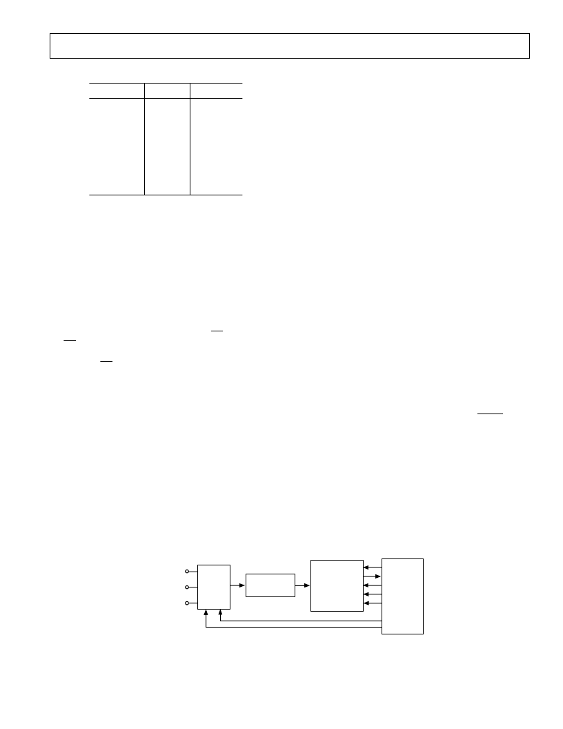
SYSTEM
REF HI
A
IN
SYSTEM
REF LO
ANALOG
MUX
A0
A1
SIGNAL
CONDITIONING
AD7703
SCLK
SDATA
CAL
SC1
SC2
MICRO
COMPUTER
A
IN
Figure 12. Typical Connections for System Calibration
low capacitance/voltage coefficient. T he device also achieves low
input drift through the use of chopper-stabilized techniques in
its input stage. T o ensure excellent performance over time and
temperature, the AD7703 uses digital calibration techniques
which minimize offset and gain error to typically
±
4 LSBs.
AUT OC ALIBRAT ION
T he AD7703 offers both self-calibration and system-calibration
facilities. For calibration to occur, the on-chip microcontroller
must record the modulator output for two different input condi-
tions. T hese are the “zero scale” and “full scale” points. In uni-
polar self-calibration mode, the zero scale point is V
AGND
and
the full-scale point is V
REF
. With these readings the microcon-
troller can calculate the gain slope for the input to output trans-
fer function of the converter. In unipolar mode the slope factor
is determined by dividing the span between zero and full scale
by 2
20
. In bipolar mode it is determined by dividing the span by
2
19
since the inputs applied represent only half the total codes.
In both unipolar and bipolar modes the slope factor is saved and
used to calculate the binary output code when an analog input is
applied to the device. T able IV gives the output code size after
calibration.
System calibration allows the AD7703 to compensate for system
gain and offset errors. A typical circuit where this might be used
is shown in Figure 12.
System calibration performs the same slope factor calculations
as self-calibration but uses voltage values presented by the
system to the A
IN
pin for the zero and full-scale points. T here
are two system calibration modes.
T he first mode offers system level calibration for system offset
and system gain. T his is a two step operation. T he zero-scale
point must be presented to the converter first. It must be
applied to the converter before the calibration step is initiated
and remain stable until the step is complete. T he
DRDY
output
from the device will signal when the step is complete by going
low. After the zero-scale point is calibrated the full-scale point is
applied and the second calibration step is initiated. Again the
voltage must remain stable throughout the calibration step.
T he two step calibration mode offers another feature. After the
sequence has been completed, additional offset calibrations can
be performed by themselves to adjust the zero reference point to
a new system zero reference value. T his second system
calibration mode uses an input voltage for the zero-scale
calibration point but uses the V
REF
value for the full-scale point.
相關PDF資料 |
PDF描述 |
|---|---|
| AD7703AR | LC2MOS 20-Bit A/D Converter |
| AD7703BN | LC2MOS 20-Bit A/D Converter |
| AD7703BQ | LC2MOS 20-Bit A/D Converter |
| AD7703BR | ECONOLINE: REC2.2-S_DRW(Z)/H* - 2.2W DIP Package- 1kVDC Isolation- Regulated Output- 4.5-9V, 9-18V, 18-36V, 36-72V Wide Input Range 2 : 1- UL94V-0 Package Material- Continuous Short Circiut Protection- Cost Effective- 100% Burned In- Efficiency to 84% |
| AD7703CN | LC2MOS 20-Bit A/D Converter |
相關代理商/技術參數 |
參數描述 |
|---|---|
| AD7703AR | 功能描述:IC ADC 20BIT LC2MOS 20-SOIC RoHS:否 類別:集成電路 (IC) >> 數據采集 - 模數轉換器 系列:- 標準包裝:1 系列:- 位數:14 采樣率(每秒):83k 數據接口:串行,并聯 轉換器數目:1 功率耗散(最大):95mW 電壓電源:雙 ± 工作溫度:0°C ~ 70°C 安裝類型:通孔 封裝/外殼:28-DIP(0.600",15.24mm) 供應商設備封裝:28-PDIP 包裝:管件 輸入數目和類型:1 個單端,雙極 |
| AD7703AR-REEL | 功能描述:IC ADC 20BIT LC2MOS MONO 20-SOIC RoHS:否 類別:集成電路 (IC) >> 數據采集 - 模數轉換器 系列:- 標準包裝:1 系列:- 位數:14 采樣率(每秒):83k 數據接口:串行,并聯 轉換器數目:1 功率耗散(最大):95mW 電壓電源:雙 ± 工作溫度:0°C ~ 70°C 安裝類型:通孔 封裝/外殼:28-DIP(0.600",15.24mm) 供應商設備封裝:28-PDIP 包裝:管件 輸入數目和類型:1 個單端,雙極 |
| AD7703ARZ | 功能描述:IC ADC 20BIT LC2MOS 20-SOIC RoHS:是 類別:集成電路 (IC) >> 數據采集 - 模數轉換器 系列:- 標準包裝:1 系列:- 位數:14 采樣率(每秒):83k 數據接口:串行,并聯 轉換器數目:1 功率耗散(最大):95mW 電壓電源:雙 ± 工作溫度:0°C ~ 70°C 安裝類型:通孔 封裝/外殼:28-DIP(0.600",15.24mm) 供應商設備封裝:28-PDIP 包裝:管件 輸入數目和類型:1 個單端,雙極 |
| AD7703BN | 功能描述:IC ADC 20BIT LC2MOS 20-DIP RoHS:否 類別:集成電路 (IC) >> 數據采集 - 模數轉換器 系列:- 產品培訓模塊:Lead (SnPb) Finish for COTS Obsolescence Mitigation Program 標準包裝:2,500 系列:- 位數:12 采樣率(每秒):3M 數據接口:- 轉換器數目:- 功率耗散(最大):- 電壓電源:- 工作溫度:- 安裝類型:表面貼裝 封裝/外殼:SOT-23-6 供應商設備封裝:SOT-23-6 包裝:帶卷 (TR) 輸入數目和類型:- |
| AD7703BNZ | 功能描述:IC ADC 20BIT LC2MOS MONO 20DIP RoHS:是 類別:集成電路 (IC) >> 數據采集 - 模數轉換器 系列:- 其它有關文件:TSA1204 View All Specifications 標準包裝:1 系列:- 位數:12 采樣率(每秒):20M 數據接口:并聯 轉換器數目:2 功率耗散(最大):155mW 電壓電源:模擬和數字 工作溫度:-40°C ~ 85°C 安裝類型:表面貼裝 封裝/外殼:48-TQFP 供應商設備封裝:48-TQFP(7x7) 包裝:Digi-Reel® 輸入數目和類型:4 個單端,單極;2 個差分,單極 產品目錄頁面:1156 (CN2011-ZH PDF) 其它名稱:497-5435-6 |
發布緊急采購,3分鐘左右您將得到回復。