- 您現(xiàn)在的位置:買賣IC網(wǎng) > PDF目錄373913 > AD7705BR (ANALOG DEVICES INC) ECONOLINE: REC2.2-S_DRW(Z)/H* - 2.2W DIP Package- 1kVDC Isolation- Regulated Output- 4.5-9V, 9-18V, 18-36V, 36-72V Wide Input Range 2 : 1- UL94V-0 Package Material- Continuous Short Circiut Protection- Cost Effective- 100% Burned In- Efficiency to 84% PDF資料下載
參數(shù)資料
| 型號(hào): | AD7705BR |
| 廠商: | ANALOG DEVICES INC |
| 元件分類: | ADC |
| 英文描述: | ECONOLINE: REC2.2-S_DRW(Z)/H* - 2.2W DIP Package- 1kVDC Isolation- Regulated Output- 4.5-9V, 9-18V, 18-36V, 36-72V Wide Input Range 2 : 1- UL94V-0 Package Material- Continuous Short Circiut Protection- Cost Effective- 100% Burned In- Efficiency to 84% |
| 中文描述: | 2-CH 16-BIT DELTA-SIGMA ADC, SERIAL ACCESS, PDSO16 |
| 封裝: | 0.300 INCH, MS-013AA, SOIC-16 |
| 文件頁數(shù): | 22/32頁 |
| 文件大小: | 264K |
| 代理商: | AD7705BR |
第1頁第2頁第3頁第4頁第5頁第6頁第7頁第8頁第9頁第10頁第11頁第12頁第13頁第14頁第15頁第16頁第17頁第18頁第19頁第20頁第21頁當(dāng)前第22頁第23頁第24頁第25頁第26頁第27頁第28頁第29頁第30頁第31頁第32頁
AD7705/AD7706
–22–
REV. A
Placing the part in standby mode reduces the total current to
9
μ
A typical with V
DD
= 5 V and 4
μ
A with V
DD
= 3 V when the
part is operated from an external master clock provided this
master clock is stopped. If the external clock continues to run in
standby mode, the standby current increases to 150
μ
A typical
with 5 V supplies and 75
μ
A typical with 3.3 V supplies. If a
crystal or ceramic resonator is used as the clock source, the total
current in standby mode is 400
μ
A typical with 5 V supplies and
90
μ
A with 3.3 V supplies. This is because the on-chip oscillator
circuit continues to run when the part is in its standby mode.
This is important in applications where the system clock is pro-
vided by the AD7705/AD7706’s clock, so that the AD7705/
AD7706 produces an uninterrupted master clock even when it is
in its standby mode.
Accuracy
Sigma-Delta ADCs, like VFCs and other integrating ADCs, do
not contain any source of nonmonotonicity and inherently offer
no missing codes performance. The AD7705/AD7706 achieves
excellent linearity by the use of high quality, on-chip capacitors,
which have a very low capacitance/voltage coefficient. The de-
vice also achieves low input drift through the use of chopper-
stabilized techniques in its input stage. To ensure excellent
performance over time and temperature, the AD7705/AD7706
uses digital calibration techniques that minimize offset and gain
error.
Drift Considerations
The AD7705/AD7706 uses chopper stabilization techniques to
minimize input offset drift. Charge injection in the analog
switches and dc leakage currents at the sampling node are the
primary sources of offset voltage drift in the converter. The dc
input leakage current is essentially independent of the selected
gain. Gain drift within the converter depends primarily upon
the temperature tracking of the internal capacitors. It is not
affected by leakage currents.
Measurement errors due to offset drift or gain drift can be
eliminated at any time by recalibrating the converter. Using
the system calibration mode can also minimize offset and gain
errors in the signal conditioning circuitry. Integral and differen-
tial linearity errors are not significantly affected by temperature
changes.
POWER SUPPLIES
The AD7705/AD7706 operates with a V
DD
power supply be-
tween 2.7 V and 5.25 V. While the latch-up performance of the
AD7705/AD7706 is good, it is important that power is applied
to the AD7705/AD7706 before signals at REFIN, AIN or the
logic input pins in order to avoid excessive currents. If this is not
possible, the current that flows in any of these pins should be
limited. If separate supplies are used for the AD7705/AD7706
and the system digital circuitry, the AD7705/AD7706 should be
powered up first. If it is not possible to guarantee this, current
limiting resistors should be placed in series with the logic
inputs to again limit the current. Latch-up current is greater
than 100 mA.
Supply Current
The current consumption on the AD7705/AD7706 is specified
for supplies in the range +2.7V to +3.3V and in the range +4.75V
to +5.25V. The part operates over a +2.7 V to +5.25V supply
range and the I
DD
for the part varies as the supply voltage varies
over this range. There is an internal current boost bit on the
AD7705/AD7706 that is set internally in accordance with the
operating conditions. This affects the current drawn by the
analog circuitry within these devices. Minimum power consump-
tion is achieved when the AD7705/AD7706 is operated with an
f
CLKIN
of 1 MHz or at gains of 1 to 4 with f
CLKIN
= 2.4575 MHz
as the internal boost bit is off reducing the analog current con-
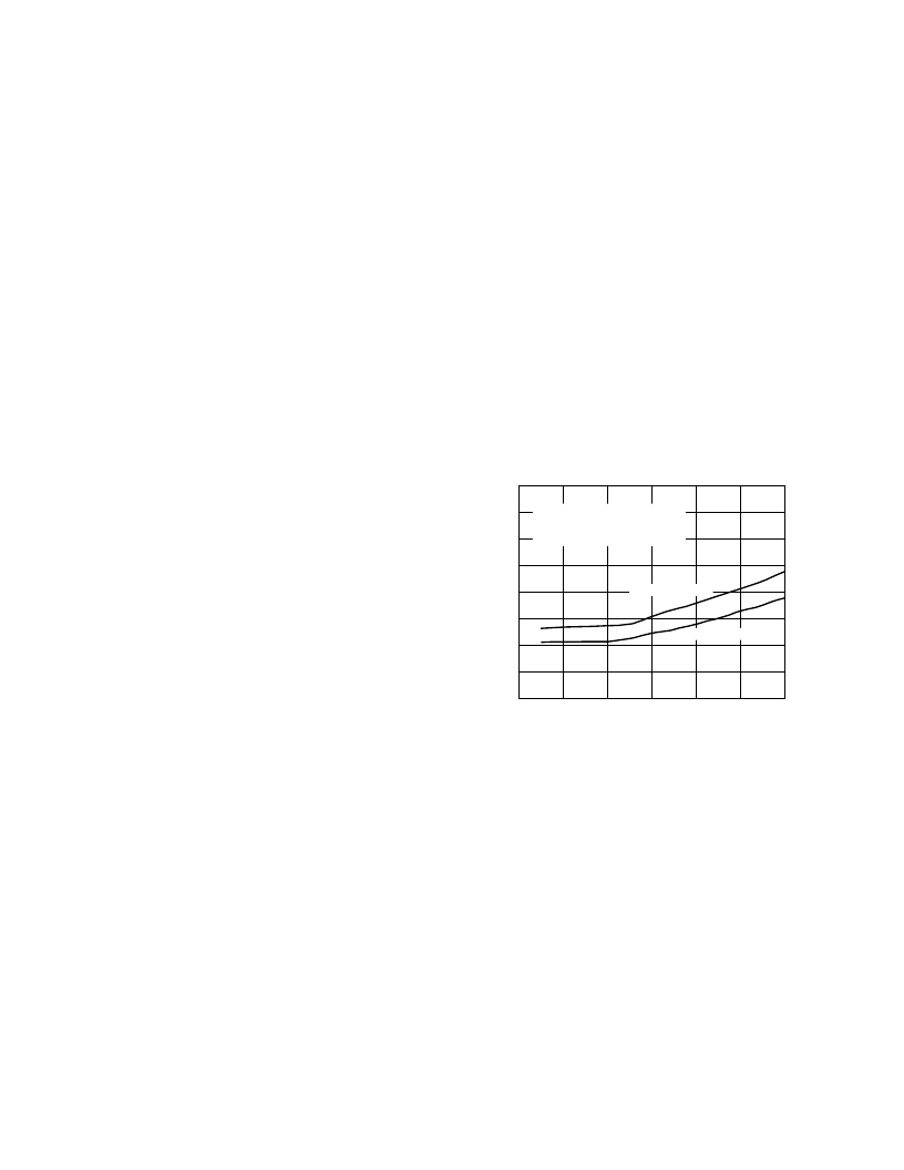
sumption. Figure 15 shows the variation of the typical I
DD
with
V
DD
voltage for both a 1MHz crystal oscillator and a 2.4576 MHz
crystal oscillator at +25
°
C. The AD7705/AD7706 is operated in
unbuffered mode. The relationship shows that the I
DD
is mini-
mized by operating the part with lower V
DD
voltages. I
DD
on the
AD7705/AD7706 is also minimized by using an external master
clock or by optimizing external components when using the
on-chip oscillator circuit. Figures 3, 4, 6 and 7 show variations
in I
DD
with gain, V
DD
and clock frequency using an external
clock.
V
DD
1600
0
2.5
I
D
m
A
1400
800
600
400
200
1200
1000
5.5
3.0
3.5
4.0
4.5
5.0
MCLK IN = CRYSTAL OSCILLATOR
T
= +25
8
C
UNBUFFERED MODE
GAIN = 128
f
CLK
= 2.4576MHz
f
CLK
= 1MHz
Figure 15. I
DD
vs. Supply Voltage
Grounding and Layout
Since the analog inputs and reference input are differential, most
of the voltages in the analog modulator are common-mode volt-
ages. The excellent common-mode rejection of the part will
remove common-mode noise on these inputs. The digital filter
will provide rejection of broadband noise on the power supplies,
except at integer multiples of the modulator sampling frequency.
The digital filter also removes noise from the analog and refer-
ence inputs provided those noise sources do not saturate the
analog modulator. As a result, the AD7705/AD7706 is more
immune to noise interference than a conventional high resolu-
tion converter. However, because the resolution of the AD7705/
AD7706 is so high, and the noise levels from the AD7705/
AD7706 so low, care must be taken with regard to grounding
and layout.
相關(guān)PDF資料 |
PDF描述 |
|---|---|
| AD7705BRU | 3 V/5 V, 1 mW 2-/3-Channel 16-Bit, Sigma-Delta ADCs |
| AD7706 | 3 V/5 V, 1 mW 2-/3-Channel 16-Bit, Sigma-Delta ADCs |
| AD7706BN | ECONOLINE: REC2.2-S_DRW(Z)/H* - 2.2W DIP Package- 1kVDC Isolation- Regulated Output- 4.5-9V, 9-18V, 18-36V, 36-72V Wide Input Range 2 : 1- UL94V-0 Package Material- Continuous Short Circiut Protection- Cost Effective- 100% Burned In- Efficiency to 84% |
| AD7706BR | 3 V/5 V, 1 mW 2-/3-Channel 16-Bit, Sigma-Delta ADCs |
| AD7706BRU | 3 V/5 V, 1 mW 2-/3-Channel 16-Bit, Sigma-Delta ADCs |
相關(guān)代理商/技術(shù)參數(shù) |
參數(shù)描述 |
|---|---|
| AD7705BR-REEL | 功能描述:IC ADC 16BIT 2CH 16-SOIC T/R RoHS:否 類別:集成電路 (IC) >> 數(shù)據(jù)采集 - 模數(shù)轉(zhuǎn)換器 系列:- 標(biāo)準(zhǔn)包裝:1,000 系列:- 位數(shù):16 采樣率(每秒):45k 數(shù)據(jù)接口:串行 轉(zhuǎn)換器數(shù)目:2 功率耗散(最大):315mW 電壓電源:模擬和數(shù)字 工作溫度:0°C ~ 70°C 安裝類型:表面貼裝 封裝/外殼:28-SOIC(0.295",7.50mm 寬) 供應(yīng)商設(shè)備封裝:28-SOIC W 包裝:帶卷 (TR) 輸入數(shù)目和類型:2 個(gè)單端,單極 |
| AD7705BR-REEL7 | 制造商:Analog Devices 功能描述:ADC Single Delta-Sigma 500sps 16-bit Serial 16-Pin SOIC W T/R |
| AD7705BRU | 功能描述:IC ADC 16BIT 2CH 16-TSSOP RoHS:否 類別:集成電路 (IC) >> 數(shù)據(jù)采集 - 模數(shù)轉(zhuǎn)換器 系列:- 標(biāo)準(zhǔn)包裝:1,000 系列:- 位數(shù):12 采樣率(每秒):300k 數(shù)據(jù)接口:并聯(lián) 轉(zhuǎn)換器數(shù)目:1 功率耗散(最大):75mW 電壓電源:單電源 工作溫度:0°C ~ 70°C 安裝類型:表面貼裝 封裝/外殼:24-SOIC(0.295",7.50mm 寬) 供應(yīng)商設(shè)備封裝:24-SOIC 包裝:帶卷 (TR) 輸入數(shù)目和類型:1 個(gè)單端,單極;1 個(gè)單端,雙極 |
| AD7705BRU-REEL | 功能描述:IC ADC 16BIT 2CH 16-TSSOP T/R RoHS:否 類別:集成電路 (IC) >> 數(shù)據(jù)采集 - 模數(shù)轉(zhuǎn)換器 系列:- 標(biāo)準(zhǔn)包裝:1,000 系列:- 位數(shù):16 采樣率(每秒):45k 數(shù)據(jù)接口:串行 轉(zhuǎn)換器數(shù)目:2 功率耗散(最大):315mW 電壓電源:模擬和數(shù)字 工作溫度:0°C ~ 70°C 安裝類型:表面貼裝 封裝/外殼:28-SOIC(0.295",7.50mm 寬) 供應(yīng)商設(shè)備封裝:28-SOIC W 包裝:帶卷 (TR) 輸入數(shù)目和類型:2 個(gè)單端,單極 |
| AD7705BRU-REEL7 | 功能描述:IC ADC 16BIT 2CH 16-TSSOP T/R RoHS:否 類別:集成電路 (IC) >> 數(shù)據(jù)采集 - 模數(shù)轉(zhuǎn)換器 系列:- 標(biāo)準(zhǔn)包裝:1,000 系列:- 位數(shù):16 采樣率(每秒):45k 數(shù)據(jù)接口:串行 轉(zhuǎn)換器數(shù)目:2 功率耗散(最大):315mW 電壓電源:模擬和數(shù)字 工作溫度:0°C ~ 70°C 安裝類型:表面貼裝 封裝/外殼:28-SOIC(0.295",7.50mm 寬) 供應(yīng)商設(shè)備封裝:28-SOIC W 包裝:帶卷 (TR) 輸入數(shù)目和類型:2 個(gè)單端,單極 |
發(fā)布緊急采購(gòu),3分鐘左右您將得到回復(fù)。