- 您現在的位置:買賣IC網 > PDF目錄373914 > AD7713* (Analog Devices, Inc.) LC2MOS Loop-Powered Signal Conditioning ADC PDF資料下載
參數資料
| 型號: | AD7713* |
| 廠商: | Analog Devices, Inc. |
| 英文描述: | LC2MOS Loop-Powered Signal Conditioning ADC |
| 中文描述: | LC2MOS回路供電ADC的信號調理 |
| 文件頁數: | 11/28頁 |
| 文件大小: | 516K |
第1頁第2頁第3頁第4頁第5頁第6頁第7頁第8頁第9頁第10頁當前第11頁第12頁第13頁第14頁第15頁第16頁第17頁第18頁第19頁第20頁第21頁第22頁第23頁第24頁第25頁第26頁第27頁第28頁
2
–11–
REV. C
AD7713
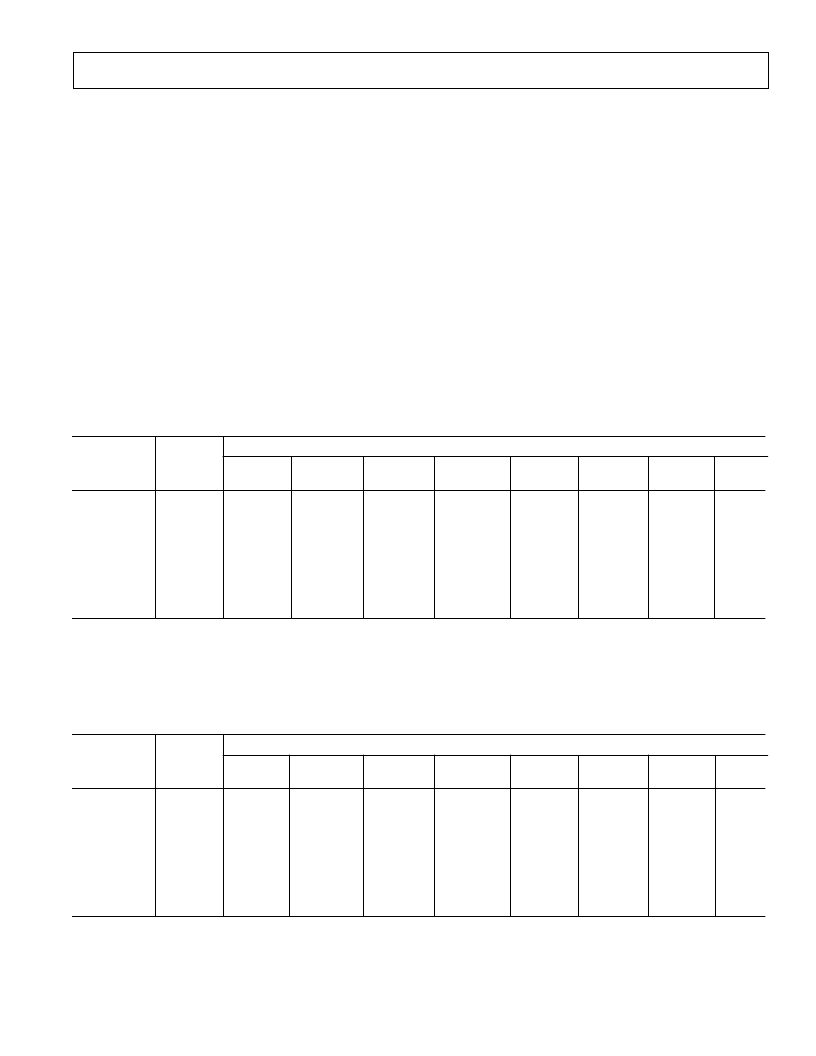
Tables I and II show the output rms noise for some typical notch and –3 dB frequencies. The numbers given are for the bipolar in-
put ranges with a V
REF
of +2.5 V. These numbers are typical and are generated with an analog input voltage of 0 V. The output
noise from the part comes from two sources. First, there is the electrical noise in the semiconductor devices used in the implementa-
tion of the modulator (device noise). Secondly, when the analog input signal is converted into the digital domain, quantization noise
is added. The device noise is at a low level and is largely independent of frequency. The quantization noise starts at an even lower
level but rises rapidly with increasing frequency to become the dominant noise source. Consequently, lower filter notch settings
(below 12 Hz approximately) tend to be device noise dominated while higher notch settings are dominated by quantization noise.
Changing the filter notch and cutoff frequency in the quantization noise dominated region results in a more dramatic improvement
in noise performance than it does in the device noise dominated region as shown in Table I. Furthermore, quantization noise is
added after the PGA, so effective resolution is independent of gain for the higher filter notch frequencies. Meanwhile, device noise is
added in the PGA and, therefore, effective resolution suffers a little at high gains for lower notch frequencies.
At the lower filter notch settings (below 12 Hz), the no missing codes performance of the device is at the 24-bit level. At the higher
settings, more codes will be missed until at 200 Hz notch setting, no missing codes performance is only guaranteed to the 12-bit
level. However, since the effective resolution of the part is 10.5 bits for this filter notch setting, this no missing codes performance
should be more than adequate for all applications.
The effective resolution of the device is defined as the ratio of the output rms noise to the input full scale. This does not remain con-
stant with increasing gain or with increasing bandwidth. Table II shows the same table as Table I except that the output is now ex-
pressed in terms of effective resolution (the magnitude of the rms noise with respect to 2
×
V
REF
/GAIN, i.e., the input full scale). It is
possible to do post filtering on the device to improve the output data rate for a given –3 dB frequency and also to further reduce the
output noise (see Digital Filtering section).
Table I. Output Noise vs. Gain and First Notch Frequency
First Notch of
Filter and O/P –3 dB
Data Rate
1
Typical Output RMS Noise (
μ
V)
Gain of
Gain of
4
8
Gain of
1
Gain of
2
Gain of
16
Gain of
32
Gain of
64
Gain of
128
Frequency
2 Hz
2
5 Hz
2
6 Hz
2
10 Hz
2
12 Hz
2
20 Hz
3
50 Hz
3
100 Hz
3
200 Hz
3
0.52 Hz
1.31 Hz
1.57 Hz
2.62 Hz
3.14 Hz
5.24 Hz
13.1 Hz
26.2 Hz
52.4 Hz
1.0
1.8
2.5
4.33
5.28
13
130
0.6
×
10
3
3.1
×
10
3
0.78
1.1
1.31
2.06
2.36
6.4
75
0.26
×
10
3
1.6
×
10
3
0.48
0.63
0.84
1.2
1.33
3.7
25
140
0.7
×
10
3
0.33
0.5
0.57
0.64
0.87
1.8
12
70
0.29
×
10
3
0.25
0.44
0.46
0.54
0.63
1.1
7.5
35
180
0.25
0.41
0.43
0.46
0.62
0.9
4
25
120
0.25
0.38
0.4
0.46
0.6
0.65
2.7
15
70
0.25
0.38
0.4
0.46
0.56
0.65
1.7
8
40
NOTES
1
The default condition (after the internal power-on reset) for the first notch of filter is 60 Hz.
2
For these filter notch frequencies, the output rms noise is primarily dominated by device noise and as a result is independent of the value of the reference voltage.
Therefore, increasing the reference voltage will give an increase in the effective resolution of the device (i.e., the ratio of the rms noise to the input full scale is
increased since the output rms noise remains constant as the input full scale increases).
3
For these filter notch frequencies, the output rms noise is dominated by quantization noise and as a result is proportional to the value of the reference voltage.
Table II. Effective Resolution vs. Gain and First Notch Frequency
First Notch of
Filter and O/P –3 dB
Data Rate
Effective Resolution
1
(Bits)
Gain of
Gain of
4
8
Gain of
1
Gain of
2
Gain of
16
Gain of
32
Gain of
64
Gain of
128
Frequency
2 Hz
5 Hz
6 Hz
10 Hz
12 Hz
20 Hz
50 Hz
100 Hz
200 Hz
0.52 Hz
1.31 Hz
1.57 Hz
2.62 Hz
3.14 Hz
5.24 Hz
13.1 Hz
26.2 Hz
52.4 Hz
22.5
21.5
21
20
20
18.5
15
13
10.5
21.5
21
21
20
20
18.5
15
13
10.5
21.5
21
20.5
20
20
18.5
15.5
13
11
21
20
20
19.5
19.5
18.5
15.5
13
11
20.5
19.5
19.5
19
19
18
15.5
13
11
19.5
18.5
18.5
18.5
18
17.5
15.5
12.5
10.5
18.5
17.5
17.5
17.5
17
17
15
12.5
10
17.5
16.5
16.5
16.5
16
16
14.5
12.5
10
NOTE
1
Effective resolution is defined as the magnitude of the output rms noise with respect to the input full scale (i.e., 2
×
V
REF
/GAIN). The above table applies for
a V
REF
of +2.5 V and resolution numbers are rounded to the nearest 0.5 LSB.
相關PDF資料 |
PDF描述 |
|---|---|
| AD7713AN | LC2MOS Loop-Powered Signal Conditioning ADC |
| AD7713AQ | LC2MOS Loop-Powered Signal Conditioning ADC |
| AD7713AR | LC2MOS Loop-Powered Signal Conditioning ADC |
| AD7713SQ | LC2MOS Loop-Powered Signal Conditioning ADC |
| AD7713 | Loop-Powered Signal Conditioning ADC(循環驅動LC2MOS信號調節A/D轉換器) |
相關代理商/技術參數 |
參數描述 |
|---|---|
| AD7713AN | 功能描述:IC ADC 24BIT SIGMA-DELTA 24-DIP RoHS:否 類別:集成電路 (IC) >> 數據采集 - 模數轉換器 系列:- 產品培訓模塊:Lead (SnPb) Finish for COTS Obsolescence Mitigation Program 標準包裝:2,500 系列:- 位數:12 采樣率(每秒):3M 數據接口:- 轉換器數目:- 功率耗散(最大):- 電壓電源:- 工作溫度:- 安裝類型:表面貼裝 封裝/外殼:SOT-23-6 供應商設備封裝:SOT-23-6 包裝:帶卷 (TR) 輸入數目和類型:- |
| AD7713ANZ | 功能描述:IC ADC 24BIT SIGMA-DELTA 24-DIP RoHS:是 類別:集成電路 (IC) >> 數據采集 - 模數轉換器 系列:- 其它有關文件:TSA1204 View All Specifications 標準包裝:1 系列:- 位數:12 采樣率(每秒):20M 數據接口:并聯 轉換器數目:2 功率耗散(最大):155mW 電壓電源:模擬和數字 工作溫度:-40°C ~ 85°C 安裝類型:表面貼裝 封裝/外殼:48-TQFP 供應商設備封裝:48-TQFP(7x7) 包裝:Digi-Reel® 輸入數目和類型:4 個單端,單極;2 個差分,單極 產品目錄頁面:1156 (CN2011-ZH PDF) 其它名稱:497-5435-6 |
| AD7713AQ | 制造商:Rochester Electronics LLC 功能描述:24 BIT SIGMA DELTA ADC IC - Bulk |
| AD7713AR | 功能描述:IC ADC SIGNAL COND LC2MOS 24SOIC RoHS:否 類別:集成電路 (IC) >> 數據采集 - 模數轉換器 系列:- 產品培訓模塊:Lead (SnPb) Finish for COTS Obsolescence Mitigation Program 標準包裝:2,500 系列:- 位數:12 采樣率(每秒):3M 數據接口:- 轉換器數目:- 功率耗散(最大):- 電壓電源:- 工作溫度:- 安裝類型:表面貼裝 封裝/外殼:SOT-23-6 供應商設備封裝:SOT-23-6 包裝:帶卷 (TR) 輸入數目和類型:- |
發布緊急采購,3分鐘左右您將得到回復。