- 您現在的位置:買賣IC網 > PDF目錄373914 > AD7714ACHIPS-5 (ANALOG DEVICES INC) 3 V/5 V, CMOS, 500 uA Signal Conditioning ADC PDF資料下載
參數資料
| 型號: | AD7714ACHIPS-5 |
| 廠商: | ANALOG DEVICES INC |
| 元件分類: | ADC |
| 英文描述: | 3 V/5 V, CMOS, 500 uA Signal Conditioning ADC |
| 中文描述: | 5-CH 24-BIT DELTA-SIGMA ADC, SERIAL ACCESS, UUC24 |
| 封裝: | DIE |
| 文件頁數: | 7/40頁 |
| 文件大小: | 306K |
| 代理商: | AD7714ACHIPS-5 |
第1頁第2頁第3頁第4頁第5頁第6頁當前第7頁第8頁第9頁第10頁第11頁第12頁第13頁第14頁第15頁第16頁第17頁第18頁第19頁第20頁第21頁第22頁第23頁第24頁第25頁第26頁第27頁第28頁第29頁第30頁第31頁第32頁第33頁第34頁第35頁第36頁第37頁第38頁第39頁第40頁
2
AD7714
REV. C
–7–
ORDERING GUIDE
AV
DD
Supply
Temperature
Range
–40
°
C to +85
°
C
–40
°
C to +85
°
C
–40
°
C to +85
°
C
–40
°
C to +85
°
C
–40
°
C to +85
°
C
–40
°
C to +85
°
C
–40
°
C to +105
°
C
–40
°
C to +105
°
C
–40
°
C to +105
°
C
–40
°
C to +85
°
C
–40
°
C to +85
°
C
Evaluation Board
Evaluation Board
Package
Option*
Model
AD7714AN-5
AD7714AR-5
AD7714ARS-5
AD7714AN-3
AD7714AR-3
AD7714ARS-3
AD7714YN
AD7714YR
AD7714YRU
AD7714AChips-5
AD7714AChips-3
EVAL-AD7714-5EB 5 V
EVAL-AD7714-3EB 3 V
5 V
5 V
5 V
3 V
3 V
3 V
3 V/5 V
3 V/5 V
3 V/5 V
5 V
3 V
N-24
R-24
RS-28
N-24
R-24
RS-28
N-24
R-24
RU-24
Die
Die
*N = Plastic DIP; R = SOIC; RS = SSOP; RU = Thin Shrink Small Outline.
TIMING CHARACTERISTICS
1, 2
(AV
DD
= DV
DD
= +2.7 V to +5.25 V; AGND = DGND = 0 V; f
CLKIN
= 2.5MHz; Input Logic 0 = 0 V,
Limit at T
MIN
, T
MAX
Parameter
(A, Y Versions)
Units
f
CLKIN3, 4
400
kHz min
Logic 1 = DV
DD
unless otherwise noted.)
Conditions/Comments
Master Clock Frequency: Crystal/Resonator or Externally
Supplied
For Specified Performance
Master Clock Input Low Time. t
CLK IN
= 1/f
CLK IN
Master Clock Input High Time
DRDY
High Time
SYNC
Pulsewidth
RESET
Pulsewidth
2.5
0.4
×
t
CLK IN
0.4
×
t
CLK IN
500
×
t
CLK IN
100
100
MHz max
ns min
ns min
ns nom
ns min
ns min
t
CLK IN LO
t
CLK IN HI
t
DRDY
t
1
t
2
Read Operation
t
3
t
4
t
56
0
0
0
80
100
100
100
0
10
60
100
100
ns min
ns min
ns min
ns max
ns max
ns min
ns min
ns min
ns min
ns max
ns max
ns max
DRDY
to
CS
Setup Time
CS
Falling Edge to SCLK Active Edge Setup Time
5
SCLK Active Edge to Data Valid Delay
5
DV
DD
= +5V
DV
DD
= +3V
SCLK High Pulsewidth
SCLK Low Pulsewidth
CS
Rising Edge to SCLK Active Edge Hold Time
5
Bus Relinquish Time after SCLK Active Edge
5
DV
DD
= +5V
DV
DD
= +3V
SCLK Active Edge to
DRDY
High
5, 8
t
6
t
7
t
8
t
97
t
10
Write Operation
t
11
t
12
t
13
t
14
t
15
t
16
0
30
20
100
100
0
ns min
ns min
ns min
ns min
ns min
ns min
CS
Falling Edge to SCLK Active Edge Setup Time
5
Data Valid to SCLK Edge Setup Time
Data Valid to SCLK Edge Hold Time
SCLK High Pulsewidth
SCLK Low Pulsewidth
CS
Rising Edge to SCLK Edge Hold Time
NOTES
1
Sample tested at +25
°
C to ensure compliance. All input signals are specified with tr = tf = 5 ns (10% to 90% of DV
DD
) and timed from a voltage level of 1.6 V.
2
See Figures 6 and 7. Timing applies for all grades.
3
CLKIN Duty Cycle range is 45% to 55%. CLKIN must be supplied whenever the AD7714 is not in standby mode. If no clock is present in this case, the device can
draw higher current than specified and possibly become uncalibrated.
4
The AD7714 is production tested with f
at 2.4576MHz (1MHz for some I
tests). It is guaranteed by characterization to operate at 400kHz.
5
SCLK active edge is falling edge of SCLK with POL = 1; SCLK active edge is rising edge of SCLK with POL = 0.
6
These numbers are measured with the load circuit of Figure 1 and defined as the time required for the output to cross the V
or V
limits.
7
These numbers are derived from the measured time taken by the data output to change 0.5V when loaded with the circuit of Figure 1. The measured number is then
extrapolated back to remove effects of charging or discharging the 100 pF capacitor. This means that the times quoted in the timing characteristics are the true bus
relinquish times of the part and as such are independent of external bus loading capacitances.
8
DRDY
returns high after the first read from the device after an output update. The same data can be read again, if required, while
DRDY
is high although care
should be taken that subsequent reads do not occur close to the next output update.
Specifications subject to change without notice.
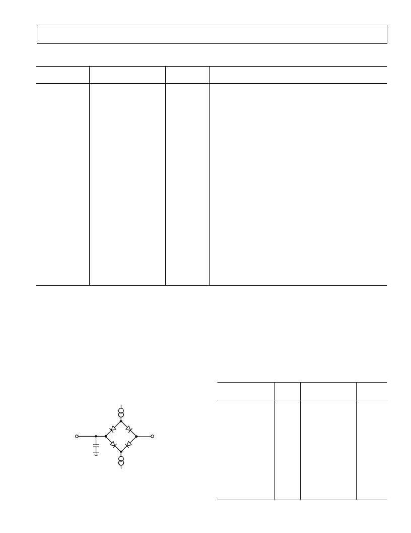
Figure 1. Load Circuit for Access Time and Bus
Relinquish Time
TO OUTPUT
PIN
50pF
I
SINK
(800
m
A AT DV
DD
= +5V
100
m
A AT DV
DD
= +3.3V)
+1.6V
I
SOURCE
(200
m
A AT DV
DD
= +5V
100
m
A AT DV
DD
= +3.3V)
相關PDF資料 |
PDF描述 |
|---|---|
| AD7714YN | 3 V/5 V, CMOS, 500 uA Signal Conditioning ADC |
| AD7714YR | 3 V/5 V, CMOS, 500 uA Signal Conditioning ADC |
| AD7714AR-3 | VARISTOR 300V RMS 14MM RADIAL |
| AD7714AR-5 | Metal Oxide Varistor (MOV); Voltage Rating AC, Vrms:680Vrms; Voltage Rating DC, Vdc:895VDC; Peak Surge Current (8/20uS), Itm:4500A; Clamping Voltage 8/20us Max :1815V; Capacitance, Cd:140pF; Package/Case:14mm Disc |
| AD7714 | Signal Conditioning ADC(信號調節A/D轉換器) |
相關代理商/技術參數 |
參數描述 |
|---|---|
| AD7714AN-3 | 制造商:Rochester Electronics LLC 功能描述:24-BIT SIGMA DELTA A/D IC - Bulk 制造商:Analog Devices 功能描述: |
| AD7714AN5 | 制造商:ANA 功能描述:24 BIT, 1KSPS, DIP 24 |
| AD7714AN-5 | 功能描述:IC ADC SIGNAL COND 5V 24-DIP RoHS:否 類別:集成電路 (IC) >> 數據采集 - 模數轉換器 系列:- 標準包裝:1,000 系列:- 位數:12 采樣率(每秒):300k 數據接口:并聯 轉換器數目:1 功率耗散(最大):75mW 電壓電源:單電源 工作溫度:0°C ~ 70°C 安裝類型:表面貼裝 封裝/外殼:24-SOIC(0.295",7.50mm 寬) 供應商設備封裝:24-SOIC 包裝:帶卷 (TR) 輸入數目和類型:1 個單端,單極;1 個單端,雙極 |
| AD7714ANZ-3 | 功能描述:IC ADC 24BIT SIGMA-DELTA 24-DIP RoHS:是 類別:集成電路 (IC) >> 數據采集 - 模數轉換器 系列:- 標準包裝:1,000 系列:- 位數:12 采樣率(每秒):300k 數據接口:并聯 轉換器數目:1 功率耗散(最大):75mW 電壓電源:單電源 工作溫度:0°C ~ 70°C 安裝類型:表面貼裝 封裝/外殼:24-SOIC(0.295",7.50mm 寬) 供應商設備封裝:24-SOIC 包裝:帶卷 (TR) 輸入數目和類型:1 個單端,單極;1 個單端,雙極 |
| AD7714ANZ-5 | 功能描述:IC ADC SIGNAL COND 5V 24-DIP RoHS:是 類別:集成電路 (IC) >> 數據采集 - 模數轉換器 系列:- 標準包裝:1 系列:microPOWER™ 位數:8 采樣率(每秒):1M 數據接口:串行,SPI? 轉換器數目:1 功率耗散(最大):- 電壓電源:模擬和數字 工作溫度:-40°C ~ 125°C 安裝類型:表面貼裝 封裝/外殼:24-VFQFN 裸露焊盤 供應商設備封裝:24-VQFN 裸露焊盤(4x4) 包裝:Digi-Reel® 輸入數目和類型:8 個單端,單極 產品目錄頁面:892 (CN2011-ZH PDF) 其它名稱:296-25851-6 |
發布緊急采購,3分鐘左右您將得到回復。