- 您現在的位置:買賣IC網 > PDF目錄373914 > AD7714AN-5 (ANALOG DEVICES INC) VARISTOR 40VRMS 1206 SMD PDF資料下載
參數資料
| 型號: | AD7714AN-5 |
| 廠商: | ANALOG DEVICES INC |
| 元件分類: | ADC |
| 英文描述: | VARISTOR 40VRMS 1206 SMD |
| 中文描述: | 5-CH 24-BIT DELTA-SIGMA ADC, SERIAL ACCESS, PDIP24 |
| 封裝: | 0.300 INCH, PLASTIC, DIP-24 |
| 文件頁數: | 14/40頁 |
| 文件大小: | 306K |
| 代理商: | AD7714AN-5 |
第1頁第2頁第3頁第4頁第5頁第6頁第7頁第8頁第9頁第10頁第11頁第12頁第13頁當前第14頁第15頁第16頁第17頁第18頁第19頁第20頁第21頁第22頁第23頁第24頁第25頁第26頁第27頁第28頁第29頁第30頁第31頁第32頁第33頁第34頁第35頁第36頁第37頁第38頁第39頁第40頁
AD7714
REV. C
–14–
ON-CHIP REGISTERS
The AD7714 contains eight on-chip registers which can be accessed via the serial port of the part. The first of these is a Communica-
tions Register which controls the channel selection, decides whether the next operation is a read or write operation and also decides
which register the next read or write operation accesses. All communications to the part must start with a write operation to the
Communications Register. After power-on or
RESET
, the device expects a write to its Communications Register. The data written
to this register determines whether the next operation to the part is a read or a write operation and also determines to which register
this read or write operation occurs. Therefore, write access to any of the other registers on the part starts with a write operation to the
Communications Register followed by a write to the selected register. A read operation from any other register on the part (including
the output data register) starts with a write operation to the Communications Register followed by a read operation from the selected
register. The communications register also controls channel selection and the
DRDY
status is also available by reading from the
Communications Register. The second register is a Mode Register which determines calibration mode and gain setting. The third
register is labelled the Filter High Register and this determines the word length, bipolar/unipolar operation and contains the upper 4
bits of the filter selection word. The fourth register is labelled the Filter Low Register and contains the lower 8 bits of the filter selec-
tion word. The fifth register is a Test Register which is accessed when testing the device. The sixth register is the Data Register from
which the output data from the part is accessed. The final registers allow access to the part’s calibration registers. The Zero Scale
Calibration Register allows access to the zero scale calibration coefficients for the selected input channel while the Full Scale Calibra-
tion Register allows access to the full scale calibration coefficients for the selected input channel. The registers are discussed in more
detail in the following sections.
Communications Register (RS2-RS0 = 0, 0, 0)
The Communications Register is an 8-bit register from which data can either be read or to which data can be written. All communi-
cations to the part must start with a write operation to the Communications Register. The data written to the Communications Reg-
ister determines whether the next operation is a read or write operation and to which register this operation takes place. Once the
subsequent read or write operation to the selected register is complete, the interface returns to where it expects a write operation to
the Communications Register. This is the default state of the interface, and on power-up or after a
RESET
, the AD7714 is in this
default state waiting for a write operation to the Communications Register. In situations where the interface sequence is lost, if a
write operation of sufficient duration (containing at least 32 serial clock cycles) takes place with DIN high, the AD7714 returns to
this default state. Table V outlines the bit designations for the Communications Register.
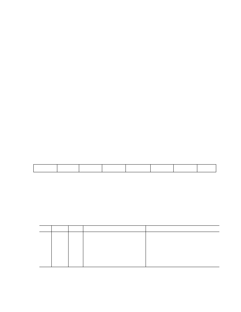
Table V. Communications Register
Table VI. Register Selection
0/
DRDY
RS2
RS1
RS0
R/
W
CH2
CH1
CH0
0/
DRDY
For a write operation, a 0 must be written to this bit so that the write operation to the Communications Register
actually takes place. If a 1 is written to this bit, the part will not clock on to subsequent bits in the register. It will stay
at this bit location until a 0 is written to this bit. Once a 0 is written to this bit, the next 7 bits will be loaded to the
Communications Register. For a read operation, this bit provides the status of the
DRDY
flag from the part. The
status of this bit is the same as the
DRDY
output pin.
Register Selection Bits. RS2 is the MSB of the three selection bits. The three bits select to which one of eight on-chip
registers the next read or write operation takes place as shown in Table VI along with the register size.
RS2–RS0
RS2
0
0
0
0
1
1
1
1
RS1
0
0
1
1
0
0
1
1
RS0
0
1
0
1
0
1
0
1
Register
Communications Register
Mode Register
Filter High Register
Filter Low Register
Test Register
Data Register
Zero-Scale Calibration Register
Full-Scale Calibration Register
Register Size
8 Bits
8 Bits
8 Bits
8 Bits
8 Bits
16 Bits or 24 Bits
24 Bits
24 Bits
相關PDF資料 |
PDF描述 |
|---|---|
| AD7714YRU | 3 V/5 V, CMOS, 500 uA Signal Conditioning ADC |
| AD7714* | 3 V/5 V. CMOS. 500 uA Signal Conditioning ADC |
| AD7714ARS-3 | 3 V/5 V, CMOS, 500 uA Signal Conditioning ADC |
| AD7714ARS-5 | 3 V/5 V, CMOS, 500 uA Signal Conditioning ADC |
| AD7714ACHIPS-3 | 3 V/5 V, CMOS, 500 uA Signal Conditioning ADC |
相關代理商/技術參數 |
參數描述 |
|---|---|
| AD7714ANZ-3 | 功能描述:IC ADC 24BIT SIGMA-DELTA 24-DIP RoHS:是 類別:集成電路 (IC) >> 數據采集 - 模數轉換器 系列:- 標準包裝:1,000 系列:- 位數:12 采樣率(每秒):300k 數據接口:并聯 轉換器數目:1 功率耗散(最大):75mW 電壓電源:單電源 工作溫度:0°C ~ 70°C 安裝類型:表面貼裝 封裝/外殼:24-SOIC(0.295",7.50mm 寬) 供應商設備封裝:24-SOIC 包裝:帶卷 (TR) 輸入數目和類型:1 個單端,單極;1 個單端,雙極 |
| AD7714ANZ-5 | 功能描述:IC ADC SIGNAL COND 5V 24-DIP RoHS:是 類別:集成電路 (IC) >> 數據采集 - 模數轉換器 系列:- 標準包裝:1 系列:microPOWER™ 位數:8 采樣率(每秒):1M 數據接口:串行,SPI? 轉換器數目:1 功率耗散(最大):- 電壓電源:模擬和數字 工作溫度:-40°C ~ 125°C 安裝類型:表面貼裝 封裝/外殼:24-VFQFN 裸露焊盤 供應商設備封裝:24-VQFN 裸露焊盤(4x4) 包裝:Digi-Reel® 輸入數目和類型:8 個單端,單極 產品目錄頁面:892 (CN2011-ZH PDF) 其它名稱:296-25851-6 |
| AD7714ANZ-5 | 制造商:Analog Devices 功能描述:A/D Converter (A-D) IC |
| AD7714AR-3 | 功能描述:IC ADC 24BIT SIGMA-DELTA 24-SOIC RoHS:否 類別:集成電路 (IC) >> 數據采集 - 模數轉換器 系列:- 標準包裝:1,000 系列:- 位數:12 采樣率(每秒):300k 數據接口:并聯 轉換器數目:1 功率耗散(最大):75mW 電壓電源:單電源 工作溫度:0°C ~ 70°C 安裝類型:表面貼裝 封裝/外殼:24-SOIC(0.295",7.50mm 寬) 供應商設備封裝:24-SOIC 包裝:帶卷 (TR) 輸入數目和類型:1 個單端,單極;1 個單端,雙極 |
| AD7714AR-3REEL | 功能描述:IC ADC 24BIT SIGMA-DELTA 24-SOIC RoHS:否 類別:集成電路 (IC) >> 數據采集 - 模數轉換器 系列:- 標準包裝:1,000 系列:- 位數:12 采樣率(每秒):300k 數據接口:并聯 轉換器數目:1 功率耗散(最大):75mW 電壓電源:單電源 工作溫度:0°C ~ 70°C 安裝類型:表面貼裝 封裝/外殼:24-SOIC(0.295",7.50mm 寬) 供應商設備封裝:24-SOIC 包裝:帶卷 (TR) 輸入數目和類型:1 個單端,單極;1 個單端,雙極 |
發布緊急采購,3分鐘左右您將得到回復。