- 您現在的位置:買賣IC網 > PDF目錄373914 > AD7714YR (ANALOG DEVICES INC) 3 V/5 V, CMOS, 500 uA Signal Conditioning ADC PDF資料下載
參數資料
| 型號: | AD7714YR |
| 廠商: | ANALOG DEVICES INC |
| 元件分類: | ADC |
| 英文描述: | 3 V/5 V, CMOS, 500 uA Signal Conditioning ADC |
| 中文描述: | 5-CH 24-BIT DELTA-SIGMA ADC, SERIAL ACCESS, PDSO24 |
| 封裝: | WSOIC-24 |
| 文件頁數: | 20/40頁 |
| 文件大小: | 306K |
| 代理商: | AD7714YR |
第1頁第2頁第3頁第4頁第5頁第6頁第7頁第8頁第9頁第10頁第11頁第12頁第13頁第14頁第15頁第16頁第17頁第18頁第19頁當前第20頁第21頁第22頁第23頁第24頁第25頁第26頁第27頁第28頁第29頁第30頁第31頁第32頁第33頁第34頁第35頁第36頁第37頁第38頁第39頁第40頁
AD7714
REV. C
–20–
ANALOG INPUT
Analog Input Ranges
The AD7714 contains six analog input pins (labelled AIN1 to
AIN6) which can be configured as either three fully differential
input channels or five pseudo-differential input channels. Bits
CH0, CH1 and CH2 of the Communications Register configure
the analog input arrangement and the channel selection is as
outlined previously in Table VII. The input pairs (either differ-
ential or pseudo-differential) provide programmable-gain, input
channels which can handle either unipolar or bipolar input
signals. It should be noted that the bipolar input signals are
referenced to the respective AIN(–) input of the input pair.
In unbuffered mode, the common-mode range of these inputs is
from AGND to AV
DD
provided that the absolute value of the analog
input voltage lies between AGND–30mV and AV
DD
+ 30mV.
This means that in unbuffered mode the part can handle both
unipolar and bipolar input ranges for all gains. In buffered
mode, the analog inputs can handle much larger source imped-
ances, but the absolute input voltage range is restricted to be-
tween AGND+ 50mV to AV
DD
– 1.5V which also places
restrictions on the common-mode range. This means that in
buffered mode there are some restrictions on the allowable gains
for bipolar input ranges. Care must be taken in setting up the
common-mode voltage and input voltage range so that the
above limits are not exceeded, otherwise there will be a degrada-
tion in linearity performance.
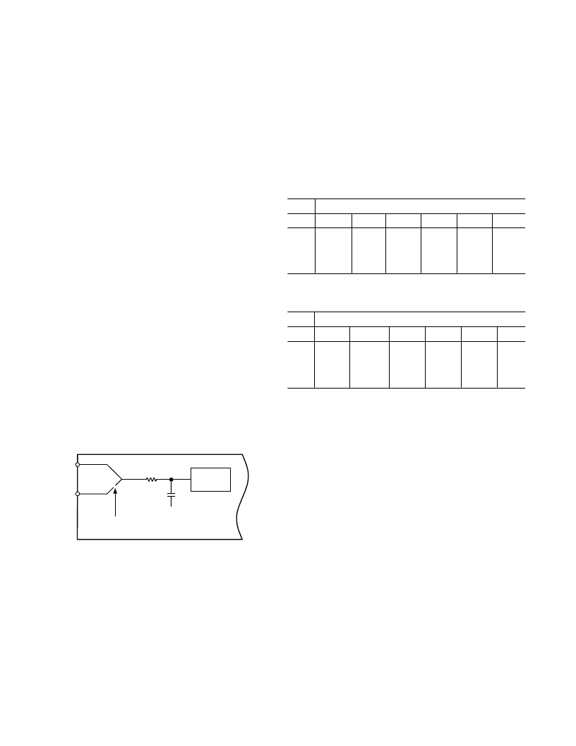
In unbuffered mode, the analog inputs look directly into the
7pF input sampling capacitor, C
SAMP
. The dc input leakage
current in this unbuffered mode is 1nA maximum. As a result,
the analog inputs see a dynamic load which is switched at the
input sample rate (see Figure 3). This sample rate depends on
master clock frequency and selected gain. C
SAMP
is charged to
AIN(+) and discharged to AIN(–) every input sample cycle.
The effective on-resistance of the switch, R
SW
, is typically 7k
.
C
SAMP
must be charged through R
SW
and through any external
source impedances every input sample cycle. Therefore, in unbuf-
fered mode, source impedances mean a longer charge time for
C
SAMP
and this may result in gain errors on the part. Table XII
shows the allowable external resistance/capacitance values, for
unbuffered mode, such that no gain error to the 16-bit level is
introduced on the part. Table XIII shows the allowable external
resistance/capacitance values, once again for unbuffered mode,
such that no gain error to the 20-bit level is introduced.
Table XII. External R, C Combination for No 16-Bit Gain
Error (Unbuffered Mode Only)
Gain
External Capacitance (pF)
0
368 k
177.2 k
44.2 k
26.4 k
82.8 k
21.2 k
12.6 k
35.2 k
9.6 k
50
90.6 k
54.2 k
100
500
14.6 k
7.2 k
3.4 k
1.58 k
1000
8.2 k
4 k
1.94 k
540
880
5000
2.2 k
1.12 k
1
2
4
8–128
5.8 k
240
Table XIII. External R, C Combination for No 20-Bit Gain
Error (Unbuffered Mode Only)
Gain
External Capacitance (pF)
0
50
100
500
1000
5000
1
2
4
8–128
290 k
141 k
63.6 k
26.8 k
69 k
33.8 k
16 k
7.2 k
40.8 k
20 k
9.6 k
4.4 k
10.4 k
5 k
2.4 k
1.1 k
5.6 k
2.8 k
1.34 k
340
600
1.4 k
700
160
In buffered mode, the analog inputs look into the high impedance
inputs stage of the on-chip buffer amplifier. C
SAMP
is charged via
this buffer amplifier such that source impedances do not affect
the charging of C
SAMP
. This buffer amplifier has an offset leak-
age current of 1nA. In this buffered mode, large source imped-
ances result in a dc offset voltage developed across the source
impedance but not in a gain error.
Input Sample Rate
The modulator sample frequency for the AD7714 remains at
f
CLKIN
/128 (19.2kHz @ f
CLK IN
= 2.4576MHz) regardless of
the selected gain. However, gains greater than 1 are achieved
by a combination of multiple input samples per modulator cycle
and a scaling of the ratio of reference capacitor to input capaci-
tor. As a result of the multiple sampling, the input sample rate
of the device varies with the selected gain (see Table XIV). In
buffered mode, the input is buffered before the input sampling
capacitor. In unbuffered mode, where the analog input looks
directly into the sampling capacitor, the effective input imped-
ance is 1/C
SAMP
×
f
S
where C
SAMP
is the input sampling capaci-
tance and f
S
is the input sample rate.
R
SW
(7k
V
TYP)
HIGH
IMPEDANCE
>1G
V
C
(7pF )
V
BIAS
SWITCHING FREQUENCY DEPENDS ON
f
CLKIN
AND SELECTED GAIN
AIN(+)
AIN(–)
Figure 3. Unbuffered Analog Input Structure
相關PDF資料 |
PDF描述 |
|---|---|
| AD7714AR-3 | VARISTOR 300V RMS 14MM RADIAL |
| AD7714AR-5 | Metal Oxide Varistor (MOV); Voltage Rating AC, Vrms:680Vrms; Voltage Rating DC, Vdc:895VDC; Peak Surge Current (8/20uS), Itm:4500A; Clamping Voltage 8/20us Max :1815V; Capacitance, Cd:140pF; Package/Case:14mm Disc |
| AD7714 | Signal Conditioning ADC(信號調節A/D轉換器) |
| AD7715ARU-3 | 3 V/5 V, 450 uA 16-Bit, Sigma-Delta ADC |
| AD7715ARU-5 | AB 4C 4#12 PIN RECP |
相關代理商/技術參數 |
參數描述 |
|---|---|
| AD7714YR-REEL | 制造商:Analog Devices 功能描述:ADC Single Delta-Sigma 1ksps 24-bit Serial 24-Pin SOIC W T/R 制造商:Analog Devices 功能描述:ADC SGL DELTA-SIGMA 1KSPS 24BIT SERL 24SOIC W - Tape and Reel |
| AD7714YR-REEL7 | 制造商:Analog Devices 功能描述:ADC Single Delta-Sigma 1ksps 24-bit Serial 24-Pin SOIC W T/R 制造商:Analog Devices 功能描述:ADC SGL DELTA-SIGMA 1KSPS 24BIT SERL 24SOIC W - Tape and Reel |
| AD7714YRU | 功能描述:IC ADC SIGNAL COND 3/5V 24-TSSOP RoHS:否 類別:集成電路 (IC) >> 數據采集 - 模數轉換器 系列:- 標準包裝:1,000 系列:- 位數:12 采樣率(每秒):300k 數據接口:并聯 轉換器數目:1 功率耗散(最大):75mW 電壓電源:單電源 工作溫度:0°C ~ 70°C 安裝類型:表面貼裝 封裝/外殼:24-SOIC(0.295",7.50mm 寬) 供應商設備封裝:24-SOIC 包裝:帶卷 (TR) 輸入數目和類型:1 個單端,單極;1 個單端,雙極 |
| AD7714YRU-REEL | 制造商:Analog Devices 功能描述:ADC Single Delta-Sigma 1ksps 24-bit Serial 24-Pin TSSOP T/R 制造商:Analog Devices 功能描述:ADC SGL DELTA-SIGMA 1KSPS 24BIT SERL 24TSSOP - Tape and Reel |
| AD7714YRU-REEL7 | 功能描述:IC ADC 24BIT SIGMA-DELTA 24TSSOP RoHS:否 類別:集成電路 (IC) >> 數據采集 - 模數轉換器 系列:- 標準包裝:1,000 系列:- 位數:12 采樣率(每秒):300k 數據接口:并聯 轉換器數目:1 功率耗散(最大):75mW 電壓電源:單電源 工作溫度:0°C ~ 70°C 安裝類型:表面貼裝 封裝/外殼:24-SOIC(0.295",7.50mm 寬) 供應商設備封裝:24-SOIC 包裝:帶卷 (TR) 輸入數目和類型:1 個單端,單極;1 個單端,雙極 |
發布緊急采購,3分鐘左右您將得到回復。